Sustainability is no longer a choice in the electronics industry – it’s an urgent priority. As businesses and regulators push for greener solutions, the conversation around circularity in PCBs (printed circuit boards) has gained momentum. While achieving full circularity remains complex, significant progress has been made in sustainable materials and recycling innovations.
We have been driving this change since 2002 (when our first environmental policy was implemented) and have conducted rigorous audits and working to lower emissions across Scope 1, 2, and 3. However, we know there’s always more to do. The challenges ahead require ongoing innovation, transparency, and collaboration – and we’re committed to leading the way.
A complex material combination
Achieving circularity in PCBs entails selecting eco-friendly materials, optimizing manufacturing processes, and ensuring effective end-of-life recycling. However, given the complex combination of fiberglass, resin, and copper in PCBs, the industry must overcome substantial hurdles to achieve full circularity. Material selection is a fundamental aspect of sustainable PCB development. Alongside industry partners, we are actively testing alternative materials that enhance recyclability, reduce environmental impact, and align with circularity principles.
Key innovations include:
- Recyclad – A recyclable FR-4 alternative containing recycled content. Our tests have shown that it offers performance comparable to halogen-free laminates like SYTECH S1150G, making it a viable step toward more sustainable PCBs. We have also been able to prove that the material is great for simpler, double-sided and multi-layer up to twelve-layer boards, but not for HDIs at this point.

- Soluboard – a bio-based PCB material developed by Jiva Materials – is made from jute fiber and a biodegradable polymer that dissolves in hot water. This allows for easy recovery of electronic components and dramatically reduces e-waste. We tested Soluboard in PCB manufacturing, low-temperature soldering, and automated assembly. While the material has some limitations – such as lower soldering temperature tolerance, lower peel strength, and mechanical strength – it remains a promising, environmentally friendly option for applications with lower requirements for material strength and reliability. We will continue to follow Soluboard’s development as it moves toward a more robust material suitable for more than 2 layers.


In autumn 2024, NCAB ordered samples of Soluboard. The material underwent standard IPC evaluation and testing by Hytek Laboratories, followed by assembly and low-temperature soldering trials. It is important to note that Soluboard is not comparable to FR-4; we must evaluate it based on its own merits rather than against fully qualified FR-4 material.
- Papershell & CirEl – These Swedish R&D initiatives explore the potential of paper-based PCB substrates. We have tested a few surface finishes (ENIG and OSP), as well as low temperature soldering and copper adhesion. While still in early development, these materials represent a major shift toward renewable alternatives.

Similar to Soluboard, the Swedish R&D Papershell and CirEl Paper materials are environmentally friendly. When fully developed, they are said to have properties similar to Soluboard.
- Bamboo and Wood-Based PCBs – Several ongoing projects investigate fast-growing, sustainable resources like bamboo and engineered wood as potential PCB substrates.
- Bio-based Epoxy Resins – Recent developments in bio-resins, such as those from Sicomin, are pushing PCB manufacturing toward greener chemistry.
Testing, testing and testing
Sustainability in PCBs isn’t theoretical; it requires real-world testing. We have been conducting trials with recyclable laminates since May 2023, with results indicating compliance with IPC-A-600 standards. Thermal stability, pad adhesion, and material degradation remain key focus areas for improvement. Challenges such as drilling precision and copper adhesion at lower soldering temperatures are also being addressed in ongoing research. These findings not only guide our partnerships on material development but also play a crucial role in shaping a more standardized approach to sustainability measurement.
To build on our material testing efforts and quantify sustainability progress, we are developing a Sustainability Rating based on Lifecycle Assessment (LCA). This framework evaluates the environmental impact of different PCB technologies, materials, and manufacturing processes while also assessing energy and water consumption throughout production. Additionally, it tracks waste generation and explores potential recycling opportunities. Working in collaboration with Cranfield University, IMEC and others, we are refining a sustainability scorecard that enables customers to make informed, data-driven decisions – ensuring a balance between performance and environmental responsibility.
Circularity and recycling
Understanding and quantifying sustainability starts with defining what we mean by circularity. This can involve circularity in PCB production, returning materials back to nature at the end of their life, or creating a true closed loop where most materials are reused to produce new PCBs. Our main target is to recycle PCB materials to avoid environmental pollution and reduce our carbon footprint (CFP). This could mean using materials that biodegrade back into nature, materials repurposed for other products, or ideally materials reused for new PCBs – a goal that, unfortunately, still seems far off.
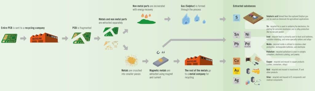
While the complexity of material separation remains a challenge, advances in recycling methods are bringing us closer to making this vision a reality. Today’s most effective recycling processes can recover up to 95% of the metals in PCBs, while resin and fiberglass can often be repurposed in other industries. Yet, despite these efforts, many PCBs still end up in landfills due to the difficulty of material separation. However, achieving a more circular PCB industry isn’t just about improving recycling – it also depends on ensuring compliance with evolving environmental regulations.
Guided by RoHS and REACH
As governments worldwide tighten restrictions on hazardous substances, manufacturers must adapt to new requirements that shape material selection and production processes. Two key frameworks shaping the industry are RoHS (Restriction of Hazardous Substances) and REACH (Registration, Evaluation, Authorization, and Restriction of Chemicals). RoHS restricts hazardous substances in electronics, particularly heavy metals like lead, cadmium, and mercury, which pose risks to both human health and the environment. Compliance ensures that PCBs meet strict safety standards, reducing toxic waste and promoting greener manufacturing. REACH, a broader European regulation, focuses on tracking and controlling chemicals used in industrial processes. It mandates manufacturers to assess and report potential risks associated with certain substances, ensuring transparency and minimizing environmental impact. As a result, PCB manufacturers must carefully monitor raw materials and processing chemicals to remain compliant.

Transition toward PFAS-free PCB manufacturing
One of the most pressing regulatory challenges today is the global effort to phase out PFAS (Per- and Polyfluoroalkyl Substances) due to their environmental persistence and health risks. PFAS, often called “forever chemicals,” were widely used in PCB laminates, coatings, and high-frequency materials because of their resistance to heat, water, and chemicals. However, their inability to break down in nature and their links to serious health risks have led to growing concerns, prompting regulatory bodies worldwide – including the EU, U.S., and Canada – to impose restrictions and bans. PFAS include over 12,000 substances categorized into three main types: PFOA, PFOS, and PTFE. Many directives, such as REACH, POPs (Persistent Organic Pollutants), CEPA (Canadian Environmental Protection Act), and TSCA (Toxic Substances Control Act), have already banned PFOA and PFOS, which are no longer used in PCBs according to our investigations with our factories. However, PTFE – commonly found in high-frequency PCB materials from manufacturers like Rogers, Taconic, and Arlon – remains under review, with the EU considering a ban by 2027.
A structured compliance process
NCAB has a structured compliance process to ensure we meet all evolving regulatory requirements. While PTFE-free alternatives are not yet available for all high-frequency applications, we have listed all materials containing PTFE, compared with none-PTFE materials with the same key parameters such as dielectric constant and material loss factor, and made the report available for our Field Application Engineers to discuss and find solutions for our customers. We are actively monitoring material developments and collaborating with suppliers to identify viable replacements. For standard PCBs that do not require PTFE-based materials, there are already many alternative options. As regulations evolve, we remain committed to leading the transition toward PFAS-free PCB manufacturing, ensuring both compliance and performance for our customers.
Achieving true circularity will require sustained investment, continuous innovation, and collaboration across the industry. We are committed to working with material suppliers to develop fully recyclable PCB substrates, expanding Lifecycle Assessment models to provide a deeper understanding of sustainability at every stage, and guiding manufacturers and customers toward eco-friendly designs that reduce waste. Compliance with RoHS, REACH, and PFAS regulations is not just about meeting requirements – it’s about reshaping the industry for long-term sustainability.
The future of sustainable PCBs won’t be defined by one single breakthrough but by a series of incremental improvements, partnerships, and a shared commitment to reshaping the industry. Circularity in PCBs is not just a goal – it’s an ongoing journey. If you’re looking for a partner dedicated to innovation, sustainability, and performance, we are here to help. Together, we can advance a future where technology and environmental responsibility go hand in hand.