Electromagnetic interference (EMI) is part of our everyday environment. It affects every electronic product — from consumer devices to advanced industrial systems.
For example, placing two microphones too close together in a karaoke room can cause noise. Similarly, in areas with chaotic geomagnetic fields, GPS positioning may become erratic or even fail entirely. Both are examples of EMI in real-world scenarios.
When EMI issues arise, they rarely occur by accident. In most cases, the root cause can be traced back to one critical component: the PCB.
Yet electromagnetic compatibility (EMC) is still often treated as “an issue only addressed during final product testing”. In reality, the roots of EMC problems are largely determined during the PCB design and manufacturing stages.
Why the PCB plays a central role
The PCB is the physical carrier of electronic devices signals, power sources, current loops, and reference planes. It is where electromagnetic noise is highly concentrated within a few functional modules. More precisely, wherever there is rapid current change or unstable reference, electromagnetic noise will inevitably be generated.
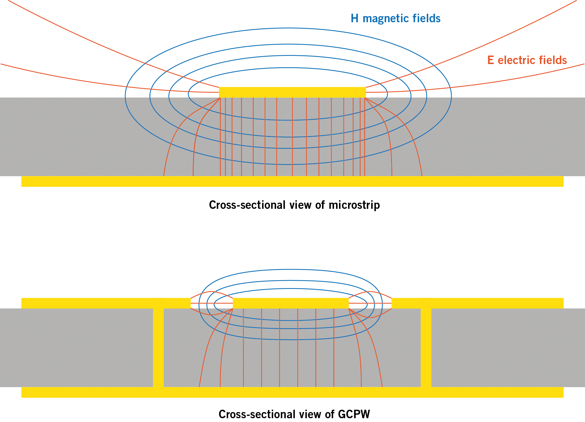
The figure below illustrates the electric and magnetic fields generated by transmission lines when power is applied to the PCB. These fields interact with surrounding signals, degrading signal quality.
Key considerations for PCB EMC design
Functional zones
A well-designed PCB separates digital, analog, and power domains clearly. Each functional block has its own noise sources, current return paths, reference requirements, and tolerable interference levels.
Without proper isolation between the blocks, the result is that return paths intersect, boundaries become unclear, and noise spreads as radiated or conducted emissions.

When placing the components on the PCB, focus on:
- Keeping high-frequency and noise-generating circuits (such as switching power supplies and clock circuits) away from sensitive circuits (such as analog signal paths and sensors) to minimize coupling of interference.
- Placing high-speed devices (such as MCUs and memory components) away from board edges and external interfaces to reduce susceptibility to external interfaces and unintended radiation.
- Placing critical components:
– Crystal oscillators and clock sources should be located as close as possible to the load devices to shorten trace lengths and reduce radiation and interference.
– Power management devices should be placed near their respective loads to minimize voltage drop and noise along the power delivery paths.
– Sensitive components (such as low-level signal amplifiers and high precision ADCs) should be positioned far from noise sources, including high-power devices and switching regulators.
In addition, the loop area of current paths must be tightly controlled, particularly for high-frequency signals. At low frequencies, a signal trace behaves primarily as a conductor; however, at high frequencies, the same trace effectively becomes an antenna. Minimizing loop area is therefore critical to reducing electromagnetic radiation.
Power and ground design
- Power plane design
The power plane should be solid and continuous. Avoid segmentation to limit the propagation of power-supply noise. Filtering capacitor should be placed at the power entry point to suppress high-frequency noise carried on the supply lines. - Ground plane design
Use a solid, continuous ground plane to provide low-impedance return paths for signals. Avoid splits, especially for high-frequency circuits, as they can lead to ground bounce and increase noise. The ground of each subsystem should be connected directly to the main ground plane through dedicated vias. - Decoupling capacitor design
Place a 0.1uF high-frequency ceramic capacitor and a 10uF bulk capacitor as close as possible to each power pin to filter high-frequency noise on the supply and to provide transient current. The ground terminal of each capacitor should be connected directly to the ground plane with a via to minimize lead inductance and improve decoupling effectiveness.
Together, the power plane, ground plane, and decoupling capacitors form a closed system that handles high-speed transient currents. The stability of this system often has a more direct impact on the overall electromagnetic performance of the PCB than the signal traces themselves.
Signal routing design
Avoid 90° right-angle corners in signal routing. Use 45° bends or curved traces instead to reduce impedance discontinuities and the resulting signal reflections.
High-speed signals (such as USB and HDMI) should be routed with controlled characteristic impedance according to design requirements (for example, 50 Ω single – ended or 100 Ω differential) to minimize signal distortion and electromagnetic radiation.
Differential signal pairs should be routed with matched trace lengths and consistent spacing to reduce skew and suppress common-mode noise.
In a microstrip configuration, signal traces are routed on the outer layers of the PCB, whereas in a stripline configuration, signals are routed between two ground planes. Stripline structures generally provide superior impedance control due to their more confined electromagnetic fields, thereby reducing susceptibility to external interference.

Crosstalk control
- High-speed signal traces (such as clocks and data buses) should follow the 3W rules (trace spacing ≥3 times the trace width) to minimize crosstalk.
- Avoid parallel routing, especially over long distances, as it increases capacitive and inductive coupling between traces.
- Guard traces connected to ground can be placed alongside critical signal lines to provide shielding and reduce susceptibility to external interference.
Other optimization measures
Layer stack-up design
A well-planned PCB stack-up is essential. Power and ground planes should be placed adjacent to each other to reduce power-supply noise coupling into signal layers. High-speed signal layers should be routed over a solid, continuous ground plane to provide a stable reference and effective shielding. A robust stack-up design helps balance impedance control, manufacturing yield, cost efficiency, and lead time.
Via design
To reduce signal distortion and electromagnetic radiation, the number of vias should be minimized, especially on critical signal paths. Via placement should be optimized to prevent the formation of large current loops or antenna effects. When high-speed signals must transition between layers, place stitching vias close to the signal via to provide a short and continuous return path.
We have seen real-world cases where the spacing between the impedance trace and the via was too close. To free up routing space between outer-layer pads, the designer proactively removed non-functional pads on the reference layer. However, the factory, considering process capabilities, enlarged the Anti-pad on the reference layer to ensure safe clearance. The result was that impedance signals did not work as expected.
From an electromagnetic perspective, enlarging the anti-pad created areas beneath the signal trace lacking a ground plane. This caused abrupt impedance changes, inducing signal reflections. Simultaneously, the enlarged anti-pad disrupted the intended return path for the signal. Consequently, the loop area formed by the signal trace and its return path increased, radiating electromagnetic energy outward and compromising the product’s EMC performance.
Material selection
PCB materials with low Dk and Df should be selected to minimize signal attenuation and distortion during transmission. Where necessary, impedance-controlled laminates or specialized coating materials can be considered to further enhance the EMC performance of the PCB.
Summary
The EMC performance of a PCB represents a trade-off among core product functionality, cost, reliability, and regulatory compliance. For example, high-speed communication equipment typically prioritizes the control of radiated emissions, whereas medical devices place greater emphasis on immunity to external interference.
PCB EMC is a broad and complex discipline, encompassing signal integrity, power integrity, thermal management, mechanical constraints, and other interrelated factors. PCB design engineers must therefore identify an optimal balance across multiple dimensions.
We recommend working closely with your PCB supplier early in the design phase to optimize each stage of the design process. This early collaboration is particularly critical for complex designs, as it helps to minimize potential risks and improve overall robustness.

Do you need help with your PCB design?
Don´t hesitate to contact us with your PCB questions.