In PCB production, time is money – but not always in the way engineers expect. A high-performance circuit design that overlooks manufacturability can bring an entire product launch to a halt. What’s more, the most expensive consequences of poor Design for Manufacturing (DfM) are often hidden in soft costs: time spent in rework, supplier back-and-forth, test failures, and unforeseen delays.
How to minimize soft costs, shorten lead times, and keep your design on track
This article highlights how common DfM pitfalls increase production lead times and non-material costs and outlines practical strategies to help design and manufacturing teams collaborate more effectively.
Soft costs: The hidden budget killers
When production stalls, it’s rarely just a material issue. Soft costs – indirect, often untracked expenses – can drive up the total cost of a board significantly. These include:
- Additional engineering time to correct DFM violations
- Back-and-forth with fabricators over ambiguous data
- Quality assurance delays due to poor testability
- Procurement setbacks due to non-standard components
- Assembly rework from layout-related issues
These issues don’t just affect the current build. They ripple into downstream production runs, warranty claims, and even reputational harm. And crucially – they delay time-to-market, where the real opportunity cost is felt.
Pitfall #1: Over-specification and tight tolerances
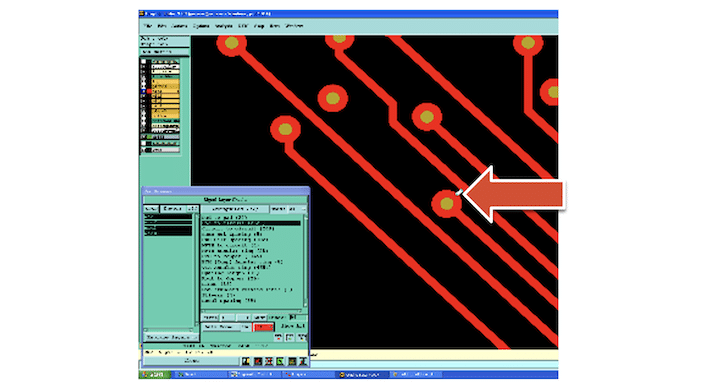
Specifying ultra-tight trace widths, spacing, or via sizes beyond a fabricator’s standard capabilities not only increases cost but also lead time.
Why it is a problem:
- Requires advanced tooling and process control.
- Causes CAM delays during design review.
- May trigger engineering change requests (EQs).
Mitigation:
Always design within the “sweet spot” of your fab house’s standard DfM guidelines unless absolutely required. Tighter tolerances should serve performance needs, not theoretical perfection.
Pitfall #2: Complex stack-ups and microvias without planning
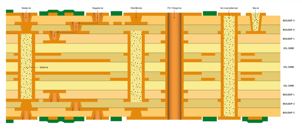
Multilayer PCBs and HDI designs are common in today’s high-density applications. But specifying blind/buried vias or non-standard layer materials without checking availability and lead time can freeze production.
How it adds cost:
- Requires specialized lamination cycles.
- Reduces vendor flexibility.
- Increases risk of scrap from layer misregistration.
Mitigation:
Coordinate with your fabricator early to review your layer stack-up. Use impedance-controlled calculators and verify material availability during layout – not after.
Pitfall #3: Incomplete or unclear fabrication documentation
Gerbers, pick-and-place files, and drill charts with missing or contradictory information are a recipe for delays.
Real Consequences:
- Manufacturers pause builds waiting for clarification.
- Adds 2–4 days to production just for issue resolution.
- May result in boards built to incorrect specs.
Mitigation:
Double-check all fabrication outputs.
Include:
- Clear net names and drill sizes
- Stack-up diagrams with materials and thicknesses
- Accurate centroid data for SMT
- Mark intended layer functions (e.g., signal, power, ground)
Pitfall #4: Poor component placement and orientation
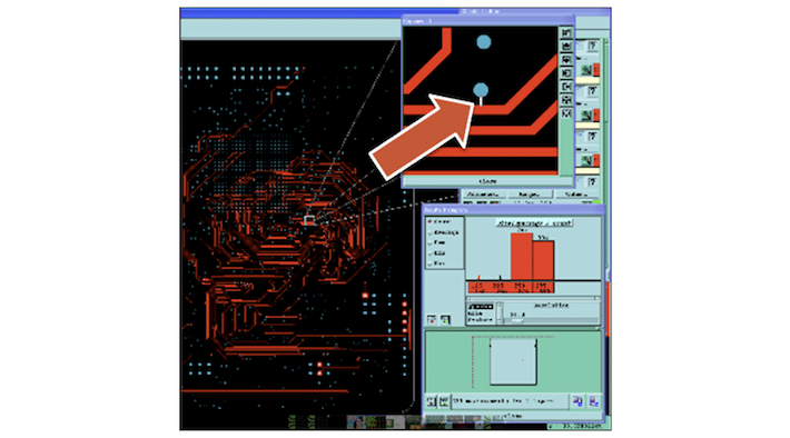
Tightly packed boards with components placed for convenience (not assembly) are a common DfM oversight. This includes misaligned polarized parts, irregular pad sizes, and minimal clearances.
Cost impact:
- Slower placement speeds or rejected placements.
- Higher likelihood of tombstoning or bridging.
- Manual inspection or rework
Mitigation:
Align polarized components consistently. Leave adequate space around BGAs or tall components. Review IPC-7351 and your assembler’s fiducial requirements during layout.
Pitfall #5: Ignoring testability (DFT)
Failure to design for test leads to higher field failures and longer debug cycles.
Hidden Soft Costs:
- Increased field service costs due to hard-to-diagnose issues.
- Delays during functional testing and validation.
- Difficulty accessing nodes for ICT or JTAG.
Mitigation:
Add test points for key signals. Ensure no parts block probe access. Include a boundary scan chain if feasible. Clearly document test coverage expectations for your EMS provider.
Pitfall #6: Using obsolete or hard-to-source components
The part may work on paper, but if it’s obsolete or has a 52-week lead time, production stalls.
Supply chain risks:
- Involuntary redesigns at the last minute.
- Secondary sourcing adds risk and inconsistency.
- Increases overall product cost due to expediting.
Mitigation:
Engage sourcing teams or EMS partners during schematic capture. Use AVL (approved vendor list) parts when possible and validate lifecycle status (via Octopart, Silicon Expert, etc.) before final BOM release.
Pitfall #7: Disregarding lead time impact of manufacturing decisions
DfM is not just about whether something can be built—it’s also about how quickly. Designing to the limits of manufacturability slows down every stage.
Lead time amplifiers:
- CAM team escalations for out-of-spec designs.
- Additional QA inspections.
- Material procurement delays (e.g., non-stock substrates).
Mitigation:
Always ask, “How long will this take to build?” as you finalize each aspect of the design—stack-up, via type, finish, copper weight. When in doubt, call your fab or EMS partner before release.
Best Practices for DFM Success
The following recommendations streamline both hard production and soft workflow costs:
| Action | Benefit |
| Early manufacturer engagement | Reduces DfM violations and changes |
| Standard stack-up and via usage | Minimizes special processes and lamination cycles |
| Comprehensive data packages | Speeds quoting and eliminates ambiguity |
| Component lifecycle checks | Prevents redesigns due to EOL/NRND parts |
| Dedicated DFM reviews | Catches errors before release and reduces ECOs |
Design guidelines ≠ Design menu: Understand what can (and can’t) be combined
As PCB design engineers, you’re used to working within tight constraints. But it’s important to understand that a capability list isn’t a menu of interchangeable features. We often see designs where customers assume they can combine, for example, Via Protection Type VI or VII with the tightest possible line/space geometries—only to end up with a board that no fabricator can build.
One common issue: a designer sees the minimum spacing for plated through-holes and then packs the board densely with vias, leaving little to no dielectric between them. This makes lamination physically impossible, as there’s not enough material left to hold the layers together.
Another case: a customer referenced our UHDI guidelines and laid out 20 µm parallel traces across the board to connect a chip, specifying hard gold on the ultra-fine bonding pads. Even the most advanced mSAP processes can’t deliver that combination. The reality is, fine-line features and hard gold are often mutually exclusive–due to both plating and dimensional tolerances.
The takeaway: capability limits are not cumulative. You need to design within the process window, not at the intersection of every extreme. Understanding how different design parameters interact – mechanically, chemically, and thermally – is just as important as knowing their individual limits. When in doubt, involve your fabricator early. It’ll save you time, cost, and a painful round of redesign.
Real-world example: How DfM slashed lead time
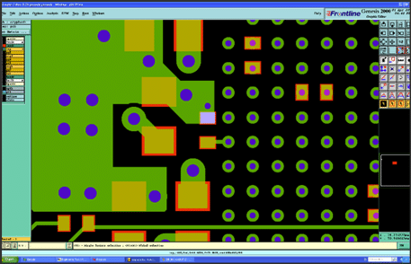
A US-based startup designed a high-density, 10-layer board with 0.075 mm microvias and blind/buried via pairs. The project hit a 6-week delay because their chosen fabricator couldn’t meet the tolerances. After consulting their EMS partner and redesigning with standard stacked vias and 0.1 mm drill sizes, production resumed in under 10 days with a 15% cost reduction.
Final thoughts
Design for Manufacturing isn’t just a checklist – it’s a mindset. The best-performing products aren’t just fast on the bench; they’re built to be fast in the factory.
By reducing DfM violations, minimizing complexity, and communicating clearly with manufacturing partners, engineers can protect schedules, reduce soft costs, and accelerate time to revenue. In a competitive electronics market, good DfM is no longer a bonus – it’s a business imperative.
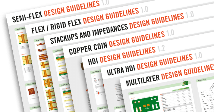
Get your design right from start with our PCB design guidelines
Design guidelines for Multilayer PCB, HDI PCB, Ultra HDI PCB, Flex / Rigid-Flex PCBs, Semi-Flex PCB, Copper coin, Via Protection, Stackups and Impedances are available for download.
