In this blog, I’ll discuss the various aspects of solder mask (also known as solder resist or solder mask varnish) for PCBs. Specifically, my focus will centre on Liquid Photo Imageable solder mask – LPI, exploring its composition, functions, and crucial considerations for both buyers and technicians involved in PCB production. Join me as I unravel the complexities of solder mask and equip you with essential insights for your manufacturing endeavours.
What is solder mask made of?
Solder mask consists of a mixture of various substances. Mainly it’s made of resin (e.g. epoxy, polyurethane, acrylic), hardener, as well as fillers, dyes, and UV-reactive substances.
- Resin and hardener are responsible for the final strength of the paint.
- The varnish manufacturer uses the fillers to optimize mechanical, thermal, and chemical resistance, among other things.
- Dyes determine the colour of the varnish.
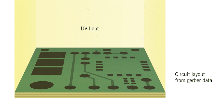
- One of the most important components is the UV absorber. This ensures that the solder mask can be photo-structured by means of UV exposure and chemical development.

What are the most important functions of solder mask?
Solder mask lives up to its name. It stops solder, thereby preventing short circuits. Common design elements to achieve this function with solder mask include:
- Bridges made of solder mask between individual solder pads. These bars prevent the pads from being short-circuited to each other due to excess solder.
- Bridges made of solder mask between solder pads, component holes and vias. This prevents solder from flowing uncontrollably from one side of the PCB to the other.
- By selectively exposing certain copper surfaces from solder mask, solder pads can be formed in e.g., ground surfaces .


Isolation
Solder mask on and between conductor traces insulates the individual conductors, prevents short circuits, and prevents leakage currents due to e.g., moisture. The dielectric strength of the solder mask layer should be at least 500V according to IPC 6012 / IPC-SM-840 .
Corrosion protection
Copper surfaces covered with solder mask are protected against environmental influences and corrosion. The coating also prevents dirt and foreign material from entering between the conductor traces during production and protects the copper surfaces from contact during the handling of the PCB, e.g., during testing and repairs.
Colours – Matte or Glossy

Solder mask is available in various colours on the market. The standard colours are green and white, for e.g., LED applications. Other common colours are red, blue, and black. In the case of green solder mask, the customer can choose between matte, semi matte, or glossy varnish.
E.g., to support the use of optical inspection systems in their production.
Visual appearance
In general, the colours of solder masks are not subject to a standard (e.g., RAL).
This is because Liquid Photo Imageable solder masks must be conditionally transparent to light, and the thickness of the coating can vary for physical and process-related reasons.
Additionally, the layout of the respective PCB influences the layer thickness of the solder mask.
Since the varnish drains conditionally off during and after coating, the coating thickness on the traces tends to be thinner than on the base material, which affects the hue of the coating.
All of these influencing factors can mean that the hue of the solder mask on the PCB can vary from production batch to production batch, which does not constitute a quality defect.
Since the solder mask is intended to have a technical rather than an optical function, the surfaces coated with solder mask do not need to be pristine. For example, slight scratches and rework on the solder mask are permissible to a limited extent. The standard IPC-A-600 specifies which optical criteria must be met for the acceptance of PCBs and which deviations are permissible. In addition, NCAB has tightened the optical acceptance criteria with the factories and only allows limited repairs to the solder mask.
Markings – Labels
Because solder mask can be easily structured photographically, it is common practice to include necessary markings (manufacturer and UL markings) and labels (part numbers, designations, date codes, notes) in the solder mask. Furthermore, positioning frames for additional labels or laser markings can easily be implemented in the solder mask.
Component holes – vias and solder mask
According to IPC-A-600, all PTH for THT components must be free of solder mask. However, this requirement does not apply to via holes, which may have residues of solder mask. According to the current state of the art, which is represented by IPC-A-600, residues of solder mask are to be expected from a via end diameter of ≤Ø0,45mm. From a final diameter of <Ø0.3mm, residues of solder mask in the via are likely.
The development of residues can range from partial coverage to complete closure of the via.
Edge coverage
NCAB requires its manufacturers to have a minimum coverage of solder mask on the edge of the trace of at least 5-8μm, depending on the base copper thickness. This is important in order to meet the requirements of IPC-SM-840 , e.g., in terms of dielectric strength.
Number of layers of solder mask
Depending on the factory, the type of varnish used, and the coating process applied, it may not be possible to achieve the necessary coverage of the trace edge with solder mask for a certain final copper thickness (50-70μm). The reason for this was already described in the section “Visual Appearance”.
The factories know their processes well and know under which conditions certain layout areas, or the entire PCB surface, need to be recoated a second time to adequately cover the trace edges with solder mask. This is referred to as a double coating.
What else is there to know about solder mask?
The solder mask process and its process steps:
- Pre-cleaning and roughening of the copper surfaces.
- Full-surface coating of both sides
- Pre-drying (before exposure) at lower temperature
- Exposure
- Development
- (UV-curing, if necessary)
- Final curing at max. temperature
Available coating processes
Liquid Photo Imageable solder mask can be applied by using the following methods.
| Procedure | Europe | Asia | Comment |
| Spray | Yes | Yes | For process engineering reasons, the factory uses only one type of paint for the spraying process (usually no selection possible). |
| Curtain casting | Yes | No | Same as above. |
| Serigraphy | No* | Yes | The factory can offer several different types of paints. *Exceptions may be made for white solder mask. |
Processes for exposure
Liquid Photo Imageable solder mask can be exposed using the following methods.
| Procedure | Europe | Asia | Comment |
| Manual Film Exposure | Yes | Yes | Due to the manual alignment of the film to copper image. Used sporadically. |
| Semi-automated film exposure | Yes | Yes | Automatic alignment of the film to the copper image, but manual material handling. Used for medium quantities. |
| Fully automated film exposure | Yes | Yes | Fully automatic material handling and alignment of the film to the copper layout. For medium to large quantities. |
| Manual Direct Imaging (Laser/LED) | Yes | Yes | Filmless direct exposure and manual material handling. Used for HDI, finer structures, smaller quantities. |
| Automated Direct Imaging (Laser/LED | Yes | Yes | Filmless direct exposure and automatic material handling. Used with HDI, finer structures, smaller quantities |
Even more about solder masks
Below, you will find further details referred to in the above text.
If this additional information does not fit to your demands, please use our design guidelines, or feel free to talk to your NCAB Engineer.
Other kinds of solder mask
Removable solder mask
With removable solder masks (also known as peelable solder masks) areas of the PCB can be covered for one or more soldering processes, so that, for example, no tin can wet these areas during eave soldering. The peelable solder mask can be manually removed after all soldering processes are completed.
The removable solder mask can cover plated-through holes within certain limits. If larger areas or larger holes need to be covered, the use of self-adhesive polyimide film can give some advantages.
Please discuss the use of removable solder mask, of self-adhesive polyimide film for your application with your NCAB technician.
Flexible solder masks
The use of flexible solder masks makes sense for certain rigid-flex and semi-flex applications.
This flexible solder mask securely covers the copper structures and accommodates the movements of the flexible layer. Alternatively, the copper can be laminated on flexible layers with coverlay foil.
Solder mask dry film
Solder mask dry film is laminated directly onto the copper surfaces and can undergo photo imaging processes.
Dry film is used for Ultra HDI and IC Substrate as well.
Solder mask material
If you need halogen-free solder mask or a halogen-free PCB, please let us know in time.
Bridges made of solder mask
If the varnish bridges between pads are too narrow, they cannot be produced reliably. Furthermore, a slight undercut can occur at the edge of the mask during production, which further reduces the surface of adhesion of the solder mask bridge to the base material.
If the web is already very narrow in the data, this can lead to a detachment of the web in combination with an undercut.
To avoid these effects, bridges of green solder mask on standard copper thickness should have a width of at least 0.1mm. For more information, see the NCAB Design Guidelines.
Solder mask defined pads
If there is a need to define solder pads in ground planes, we ask you to consider the effects of the thermal conductivity of copper surfaces on your soldering process.
For solder mask defined pads, it can be necessary to reduce the connection of the pad to the remaining copper, to prevent heat dissipation.
Acceptance standards and criteria
- Acceptance standards
The most important standards for rigid PCB with solder mask is the IPC-6012, in combination with IPC-A-600.
The standard for the solder mask itself is IPC-SM-840. For example, dielectric strength of at least 500V, as well as the differentiation of solder mask types into the classes T (telecom) and H (high reliability) are defined. NCAB specifies class T and UL94 as the minimum requirements for solder masks. Class H corresponds to Class 3 according to IPC 6012. - Visual acceptance criteria for the PCB
The visual acceptance criteria for the solder mask on the PCB are defined in IPC-A-600 (illustrated catalogue).
Solder mask varnishes, colours, selection, and approvals
Red, blue, black, and white solder mask varnishes usually have slightly different processing parameters and properties than green solder mask varnishes. This is due to the fact that different dyes and fillers are used, and that white and coloured solder mask varnishes are less translucent. This circumstance impacts exposure time and light energy for imaging and thus on the maximum resolution (smallest structure) of the corresponding solder mask type.
When selecting the solder mask, NCAB checks for:
- a.) The quality level of the solder mask according to IPC-TM-840 (NCAB requires min. class T).
- b.) The availability of required UL approvals (NCAB requires min. UL94) at the factories selected for production.
- c.) In combination with the other requirements for the PCB.
UL approvals are time-consuming and costly. That is why no factory uses all the colours and types of solder mask varnish available on the market (UL lists over 1,600 paint types).
Furthermore, no factory has UL approvals for every theoretically possible combination of layout, base material and solder mask varnish. To secure supply and process NCAB recommends that colour and type of solder mask should be discussed in advance.
Green solder mask varnish in matte or glossy
In normal applications, it makes no difference whether green solder mask is specified and used in a matte, semi-matte, or glossy finish. However, there are use cases, such as conformal coating, or appearance requirements from end-customers, where the decision if matte or glossy can make a difference for process reliability. If you or your customer likes to use e.g. conformal coating, or if your end-customer has appearance requirements, please contact us.
Markings and labels – machine-readable labels
The font size, font width, and character spacing of labels and markings in the solder mask should not be less than 125μm.
If machine-readable marking is required, close cooperation is recommended with regard to the readable content and its nomenclature, the necessary character sizes, the position, and the substrate is recommended.
Vias and solder mask residues
Solder mask residues in vias are mainly due to 3 factors.
- a.) The smaller the via diameters, the more likely they are to function like a sieve that collects larger particles. This means that the smaller the vias, the greater the risk of residue and via closure.
- b.) 2 factors are responsible for the curing of solder masks.
- The biggest factor is the exposure energy applied to the varnish, triggers polymerization and “structures” the solder mask.
- Another factor is “temperature over time”. The smaller the via, the greater the risk that the paint will start to polymerize and cure during the drying process before exposure.
- c.) Rinsing – cleaning the via in the development process becomes increasingly difficult with small diameters.
| Via End Diameter | Circle Circumference | Circle Area |
| 0,3mm | 0,942mm | 0.071mm² |
| 0,4mm | 1,257mm | 0.126mm² |
| 0,5mm | 1,571mm | 0.196mm² |
For this reason, NCAB recommends using via-protection according to IPC 4761 (type V, VI, or VII) for vias with a final diameter of ≤0.45mm for a process-reliable application of the solder mask.

PCB design guidelines
Get it right from the start with our PCB design guidelines. To prevent getting it wrong from the start, we have put together our design guidelines, to use as a checklist.
