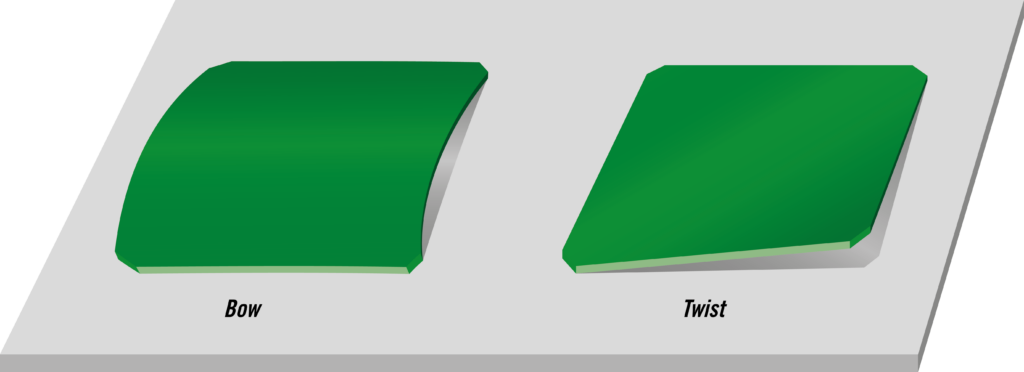
Bow and twist in PCBs are two types of deformations that can occur in the circuit board. Bow refers to there being an upward or a downward curve in the middle part of the PCB. Think of it as there being a gentle hump or arc in the middle of the board. Twist refers to there being one corner higher or lower than the other corners of a PCB board.
The development of new components has consistently acted as a catalyst propelling PCB technology to greater heights. Smaller and fine pitch footprints of Surface Mount Technology (SMT) components challenge the PCB makers to achieve High Density Interconnections, higher pattern accuracy and improved flatness. Sometimes the PCB itself becomes an SMT component that shall be soldered to a bigger PCB, which will increase the requirements further.
As a result of either components requirements or that the PCB itself becomes an SMT component, there is a challenge for both improved flatness, and to avoid bow and twist under or after assembly. This challenge has driven us further, and challenged what we can call “bow and twist management.”
As mentioned before, in the context of printed circuit board (PCB) manufacturing, “bow and twist” refers to two types of deformations that can occur in a PCB.
Both bow and twist can have negative impacts on the performance and reliability of a PCB as manufacturers want their PCBs to be perfectly flat.

The development of high-density interconnections and the integration of smaller SMT components have led to significant challenges in managing bow and twist in PCBs. This blog explores the causes of intrinsic and extrinsic bow and twist, outlines various factors contributing to these issues, and provides insights into strategies for improving PCB flatness and overall performance.
Understanding Bow and Twist in PCBs – Intrinsic and Extrinsic Bow and Twist
The concept of bow and twist in PCBs encompasses intrinsic and extrinsic factors that impact the flatness and performance of the board.
We can divide the root causes for bow and twist into two groups: Intrinsic and extrinsic bow and twist. Intrinsic bow and twist has been induced into the PCB before or during the lamination cure steps, and there are no corrective actions with permanent effect. Extrinsic bow and twist has been induced after the lamination cure steps, and corrective actions can be taken.
There are various reasons behind extrinsic and intrinsic bow and twist. Below are some examples of how production, layout and composition, and external forces and processes, can influence a boards susceptibility to bow and twist:
Production related intrinsic reasons:
- Lamination press malfunction
- Cross plying prepreg or inner layers – warp and fill directions must be same
- Wrong glass ply construction used (Prepreg or Cores)
- Missing or extra prepreg glass ply
- Weave distortion (Cores or Prepreg)
- Not fully cured inner layers
Design related intrinsic reasons:
- Non-symmetric build (Prepreg and/or Cores)
- Unbalanced copper distribution
- Layer to layer copper weights
- Within layers causing low pressure areas
- Core constructions
- Breakaway area not matching copper distribution per layer
The more you know
The copper pattern design in the breakaway area should mimic the copper distribution for each layer. If the breakaway area is perfectly balanced, it will behave differently from the non-perfect board, potentially causing stress that could lead to a twist in the panel, especially when separating the PCB from the breakaway area.
External related extrinsic reasons:
- Mechanical deformation
- Handling
- Heat during the solder mask or legend cure step.
- HASL process
- PCB assembly process
Bow and twist test procedures
The PCB manufacturer shall perform tests during the production process to prevent intrinsic bow and twist. When the PCB arrives at the customer’s side with excessive bow and twist, it is important to verify whether the root cause is intrinsic or extrinsic. We recommend the following procedure:
- Measure bow and twist by IPC TM650 2.4.22
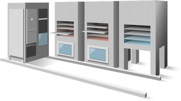
- Bake the boards 10 degrees higher than the material Tg for 20 minutes, laying them flat, side by side with no pressure or touching.
- Cool the boards to room temperature at 1 degree per minute while keeping the oven door closed.
- Measure the bow and twist again using IPC TM650 2.4.22
- The delta of bow and twist is now the degree of intrinsic and extrinsic mix.
- If the boards become completely flat, the root cause is purely extrinsic.
- If the boards stay the same, the root cause is purely intrinsic.
- Any between is a mix.
Bow and twist improvements
When addressing bow and twist issues that exceed normal tolerances, we must investigate the underlying intrinsic causes and fine-tune both design and production aspects that could impact performance. To begin, we must ensure that all relevant production processes are under control. Subsequently, we need to review potential improvements in the production process that could elevate performance beyond standard expectations.
Lamination process
The lamination process is normally tuned to be cost effective and still meet specified tolerances. The pressing cycle can be tuned further by extended cycle times to achieve improved performance.

Prepreg and inner cores
The use of prepreg is a tradeoff between a customer’s specifications and the optimal choice for high performance. To give improved stability, the build must be 100% symmetric, and we need to choose the most robust prepregs and core constructions. The result will probably affect impedance that needs to be recalculated.
Copper distribution
Copper distribution must be optimized within each layer and should be matched within the build. The build must be symmetric and all pairs of layers on each side of the build center should have equal copper weight.
Low-pressure areas
Many designs with a high layer count will have a tendency of low-pressure areas. This could be avoided by adding copper filling by dummy pads or cross hatched copper.
Split ground planes
Many PCB designs have so-called split planes that may perform as a bend indicator line, especially if we have the same pattern in more than one layer through the build.
Breakaway areas
The breakaway area is maybe the most neglected reason for bow and twist. It is essential for the performance that the copper on every layer of the breakaway area mimics the copper of the PCB itself.
Managing bend and twist for enhanced performance is a complex task that encompasses all of the aforementioned considerations. Detecting which actions yield the desired effect may necessitate several sample runs. Furthermore, various measures can be taken during the soldering and assembly process to improve flatness.
With the support of our experienced manufacturers, we possess the expertise and knowledge to guide our customers toward achieving superior performance. For assistance with such issues, please reach out to your dedicated sales contact, who will coordinate assistance from one of our application engineers.

PCB design guidelines
Get it right from the start with our PCB design guidelines. To prevent getting it wrong from the start, we have put together our design guidelines, to use as a checklist.
