Tabbed routing is an innovative PCB routing method developed by Intel to address the limited routing space on printed circuit boards (PCBs), which often cannot accommodate the required transmission line width and spacing.
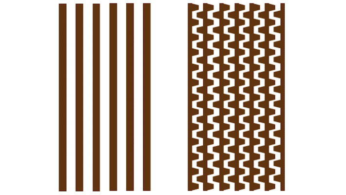
This constraint can result in impedance mismatches and significant signal crosstalk. By efficiently utilizing PCB space and incorporating small blocks called “tabs” into the transmission line structure, tabbed routing improves signal impedance matching and reduces signal crosstalk. A typical structure is shown in the diagram below. Although tabbed routing can theoretically be applied to any bus, it is primarily used in DDR (double data rate) bus applications due to the specific routing challenges associated with different bus types.
Why use tabbed routing?
Let’s look at the overall schematic of DDR PCB routing, which can be roughly divided into three parts: the CPU area, the routing area, and the DIMM connector or DRAM area. (First, it’s important to understand the wiring characteristics of the DDR bus and key concepts such as Pin Field, Breakout, and Open Field.)
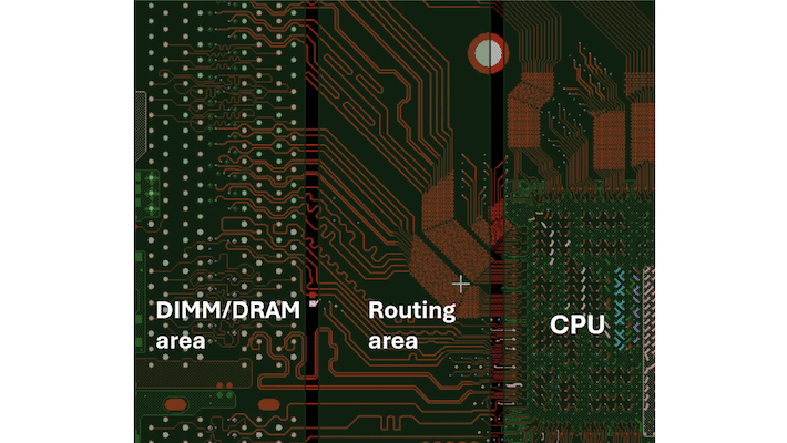
Using the diagram below as an example, expand and refine the CPU area and part of the routing area. For this PCB layout, assuming a transmission line impedance requirement of 40 ohms, which requires a line width of 6mil. To meet PDG requirements, the line spacing should be 18mil.
The pin field refers to the area surrounding the BGA balls and their corresponding vias in the CPU/BGA region. A key characteristic of this area is that a large portion of the PCB space is occupied by BGA pads and the vias connecting their traces, leaving limited room for signal routing. To accommodate all signal traces within this constrained space, narrower trace widths and reduced spacing must be used.
For example, due to the restricted area, the transmission line width is limited to 3.5 mils. Compared to the standard width of 6 mils, this results in increased impedance, creating a discontinuity in the signal path. Additionally, the line spacing tends to be more inconsistent and generally smaller—such as 4 mils—compared to the standard spacing of 18 mils, which increases signal crosstalk.

Another type of pin field is used in inner-layer stripline routing and multi-channel DDR layouts. In this approach, traces within the BGA region are routed on deeper PCB layers and can only pass between vias. Between two adjacent vias, only two signal traces can be routed, each with a width of approximately 3.5 mils and a spacing of 4 mils. This configuration results in higher impedance. In an ideal stripline setup, far-end crosstalk is expected to remain relatively low.

The section following the pin field is called the breakout field, which offers more available routing space. However, due to the high density of DDR signal lines, a dedicated area is still required to fan out the signal traces. As a result, the breakout field remains somewhat space-constrained. Typically, traces with a width of 4 mils and a spacing of 8 mils are used in this area. Compared to standard routing – 6 mil width and 18 mil spacing – this configuration results in relatively high impedance and increased signal crosstalk.
After the signal traces have fanned out in the breakout field, they enter a wider area where routing can take place, known as the open field. In this area, standard routing follows design rules, with a trace width of 6 mils and a spacing of 18 mils. In DDR design, signal reflection and crosstalk are the two primary challenges. Engineers and designers must strive to maintain consistent impedance and minimize crosstalk as much as possible.
The conventional approach in PCB design is to use standard line width and spacing wherever possible. This means that the length of the pin field and breakout field regions should be minimised. Ideally, all routing would follow the open field approach, where standard routing according to design rules can be applied. However, this is difficult to achieve in DDR PCB design, as it significantly increases cost due to the need for additional routing layers to fan out the BGA signal traces.
When wiring length in the pin field and breakout field regions cannot be minimized, Intel recommends using the tabbed routing method. This technique adds tabs in these areas to maintain consistent impedance and reduce far-end crosstalk.
Principles and simulations of tabbed routing
As mentioned above, tabbed routing serves two primary functions:
- Reduce the impedance in this area, improving impedance matching and thereby reducing signal reflection.
- Reduce crosstalk between signals, more specifically, reduce far-end crosstalk.
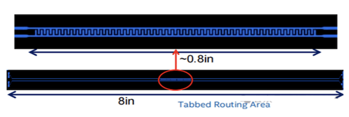
For the first point, it is quite intuitive: adding tabs increases the line width, which reduces the impedance and brings it closer to the impedance of normal routing. Simulation can be used to verify the effect of adding tabs. The following example is from Intel’s publicly released documentation. For a pair of microstrip lines, the coupling length is 8 inches.
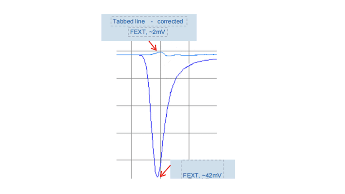
The far-end crosstalk value decreases from 42mV to 2mV when comparing the results with and without tabbed routing. However, in actual projects, due to limitations in the PCB area, the size of the tabs cannot be adjusted arbitrarily, and the results may vary.
Its role and effect can also be observed in the time-domain eye diagram.
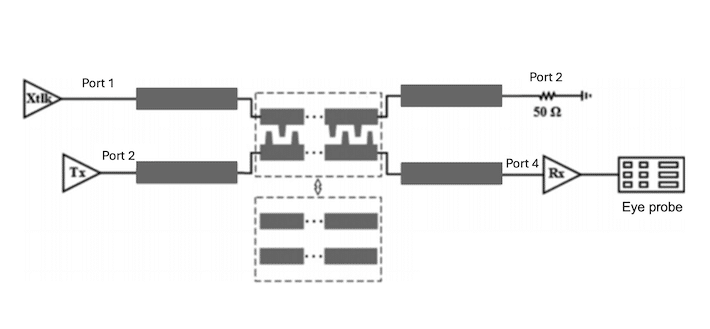
The following compares the eye diagram simulation results before and after applying tabbed routing. The results show that both eye width and eye height improve to varying degrees after the routing is added.

Tabbed routing – design and application
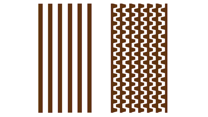
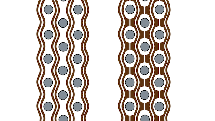
In PCB design, different types of tabs are used in different areas to optimize signal integrity and impedance matching. Below are several types of tabs and their differences:
a. Interdigital tabs (breakout field):
b. In field tabs (pin field):
c. In actual design projects, there can be various tabbed routing methods depending on the PCB shape and routing area:


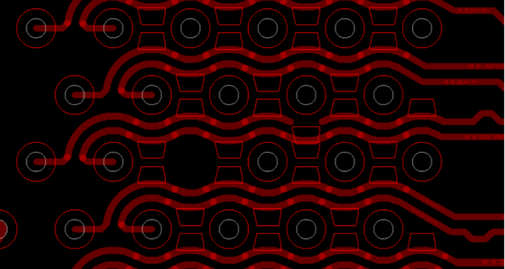
d. Tabbed routing parameters – In design projects, PCB software such as Allegro includes integrated plug-ins that allow the tabbed routing design to be completed automatically by simply entering the required parameters.
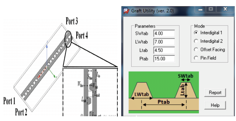
In general, facing tabs are used in both the pin field and open field to control mutual capacitance and impedance, improving signal integrity. Pin field tabs are applied specifically for impedance matching within the pin field area, while interdigital tabs mainly address trace density and crosstalk in the outer open field.
DDR tabbed routing design tips
- Consistency in the number of tabs: Within each DQ or DQS group, the number of tabs must be consistent, with a tolerance of ±1. If the breakout length of any DQ or DQS signal does not permit the use of tabbed routing, then none of the other signals in that group should use it either. This ensures uniform signal delays across the length-matched group.
- Size and spacing design: The size and spacing of tabs should be determined based on specific factors such as stack-up configuration, trace length, available routing space, and other design constraints. These parameters must be verified through simulation to ensure optimal impedance matching and effective crosstalk suppression.
Is tabbed routing suitable for particulate DDR
- Chip-based DDRs typically feature a more compact layout with a relatively short bus length. Due to their packaging and peripheral connections, they may lack a breakout area as pronounced as that found in DIMM-based DDRs.
- The pin field area of chip-based DDR typically features shorter routing lengths and a smaller region of impedance discontinuity, making impedance mismatch less of a concern compared to DIMM-based DDR. As a result, the need for tabbed routing to address impedance issues is correspondingly lower.
- The length of the pin field can vary across different DDR packages, making it difficult to standardise the number of tabs used. This variability affects signal delay consistency and increases the complexity of maintaining accurate length matching.
- Chip-based DDR offers greater flexibility in wiring methods and layer selection, and does not always require extensive surface routing. While tabbed routing provides notable advantages for crosstalk reduction and impedance control in surface routing, these benefits are less pronounced when chip-based DDR does not rely heavily on surface layers.
- Generally speaking, DIMM DDR is typically used in devices such as computers and servers with high-performance requirements and higher speeds, while chip-based DDR is more commonly used in devices with stricter space and power constraints. These devices tend to have lower speeds, and the signal integrity issues are less critical.
When using tabbed routing in PCB design, it’s important to note that tabs can increase coupling between signal lines. If placed too close to other traces, the additional copper may enhance capacitive or inductive coupling, leading to increased crosstalk. Poorly designed tabs can also resonate at certain frequencies, amplifying high-frequency noise and worsening signal integrity.
To mitigate these risks, the size, spacing, and other parameters of the tabs must be carefully optimised through simulation. This design process is more complex, and the inclusion of tabs increases PCB manufacturing difficulty, resulting in higher production costs and times.
Conclusions
Tabbed routing is an innovative design method developed by Intel for scenarios where PCB routing space is limited. It enables impedance compensation and reduces far-end crosstalk within constrained areas, thereby enhancing overall signal performance. While it is widely used in DDR PCB design, tabbed routing can also be applied in packaging, interposers, and other domains.
Although tabbed routing offers clear benefits in high-density, high-speed designs, it may not be necessary for circuits with ample routing space, lower signal rates, or less stringent signal integrity requirements. In such cases, the performance gains may not justify the added design complexity and increased manufacturing costs.
References:
1.Tabbed_Routing_Basics_563771_rev1_0, Intel
2.Cheng-Yu Tsai,etc, „Mitigate Package Level Crosstalk Using Tabbed Design”, in 2023 IEEE, 979-8-3503-8412-3
3. PCB-west-2016-new-techniques-address-layout-challenges-high-speed-routing-cp, Cadence.
Download our PCB design guidelines
And get more useful information on how to design reliable PCBs. They are available for Multilayer PCB, HDI PCB, Ultra HDI PCB, Flex / Rigid-Flex PCBs, Semi-Flex PCB, Copper coin, Via Protection and Stackups and Impedances.
