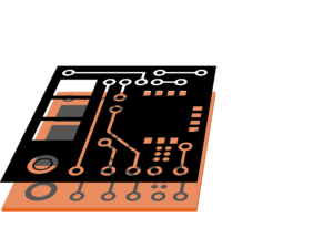
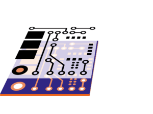
Proces produkcyjny – dla wielowarstwowych płytek PCB
Nie ma standardowych płytek drukowanych. Każda płytka jest unikalną płytką dedykowaną do konkretnego produktu. Dlatego produkcja płytki PCB to złożony proces obejmujący wiele kroków. Niniejszy przegląd obejmuje najważniejsze kroki podczas produkcji wielowarstwowej płytki PCB.
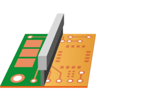
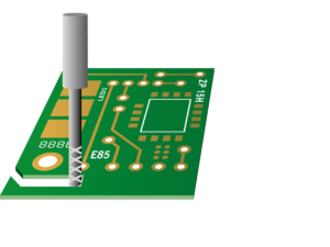
Te krótkie filmy pokazują 33 kroki w procesie produkcji płytki PCB. Zamawiając płytki PCB od NCAB Group, inwestujesz w jakość, która z czasem przyniesie korzyści. Jest to zagwarantowane przez naszą specyfikację produktu i rygorystyczną kontrolę jakości przewyższającą te stosowane przez innych dostawców, to zapewnia, że produkt spełnia najwyższe oczekiwania. Zobacz, jak wyjątkowy i wykraczający ponad standardy IPC jest proces produkcji w NCAB.
Jeśli potrzebujesz dodatkowych informacji lub pomocy, zapraszamy do kontaktu z lokalnym przedsiębiorstwem NCAB Group. Chętnie udzielimy wszelkiego wsparcia.
- NCAB Group PCB Specification is applied
- NCAB Specific production routines
- Clean room

Customer supplied Gerber data is used to generate manufacturing instructions for PCB production, including imaging and drilling. Engineers verify requirements against capabilities, define process steps, and establish checks. Any changes require NCAB Group approval.
Various materials sourced from approved suppliers are stored in controlled environments until needed. Materials are released for specific purchase orders, with base materials cut to size as required. Full traceability ensures that all materials can be linked to their manufacturing batches.
NCAB ADDED VALUE
In our factories, we build in security from the very start of the process by having dedicated pre-production engineers (PPEs) – evaluated and educated by NCAB – handling your data. These PPEs also ensure the data is handled in accordance with our demands for data integrity.
We only use internationally known base materials – we don´t allow ‘local’ or unknown brands.
The image transfer process transfers the image to the board surface using photosensitive dry film and UV light, or laser direct imaging (LDI), in a clean room. The exposed dry film polymerizes, replicating the artwork.
Next step entails developing the dry film to prepare for etching to remove unwanted copper from the panel. After etching, the remaining dry film is stripped away, leaving the designed copper circuitry.
The circuitry undergoes an Automatic Optical Inspection (AOI) against digital images to ensure accuracy and defect-free quality. Scanning identifies anomalies, verified by trained inspectors. NCAB Group does not permit repair of open circuits.
NCAB ADDED VALUE
All PCBs are tested using NCAB approved equipment and no track welding or open circuit repair is allowed. This provides increased reliability as there is no risk of repair failure, nor will this impair signal integrity.
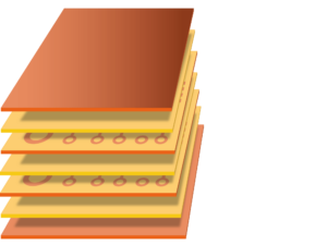
The inner layers have an oxide layer applied and are then “stacked” together with prepreg, providing insulation between layers, and copper foil is added to the top and bottom of the stack. The lamination process uses a combination of specific temperature and pressure for a specific time to allow the resin within the prepreg to flow, cure, and bond the layers together to form a solid multilayer panel.
NCAB ADDED VALUE
We only allow the factories to use materials that comply with IPC-4101 table 3-7, class B/L for max thickness and D for min thickness of dielectric.
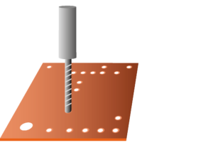
We now have to drill the holes that will subsequently create electrical connections within the multilayer PCB. This is a mechanical drilling process that must be optimised using X-ray equipment to ensure that we can achieve registration to all of the inner layer connections. The panels can be stacked at this process. The drilling can also be done by a laser drill.
NCAB ADDED VALUE
All PCBs are drilled using NCAB approved equipment which offer the best performance such as positional accuracy.
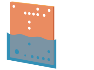
Plated through hole (PTH) involves depositing a thin layer of copper on both hole walls and the panel, ensuring electrical continuity. This process, meticulously controlled, extends copper even onto non-metallic hole walls. Following PTH, panel plating adds a thicker copper layer (typically 5 to 8 micrometers), optimizing the amount of copper for subsequent plating and etching processes to meet track and gap specifications effectively.
NCAB ADDED VALUE
To ensure quality and consistency, we have agreements in place with our factories on what chemistry shall be used.
Similar to the inner layer process of image transfer, but with a key difference: the dry film is selectively removed to define circuitry where copper will be plated later.
Additional copper is then deposited in areas without dry film, ensuring the final plating thickness meets either (i) NCAB’s requirement of an average 25μm through the hole, or (ii) aligns with the customer’s surface thickness preferences, should they have a specification beyond the NCAB requirement. Tin is then applied to protect the plated copper.
Strip Etch Strip involves: removing blue dry film, etching unwanted copper (protected by tin), and chemically removing tin to expose the final circuitry.
NCAB ADDED VALUE
NCAB provides through-hole plating of 25μm nominals as a standard (equates to IPC class 3). This is 25% more copper than achieved with IPC class 2 and provides greater reliability of the via structure and improved z-axis expansion performance.
All PCBs are tested using NCAB-approved equipment, and no track welding or open circuit repair is allowed. This provides increased reliability as there is no risk of repair failure, nor will this impair signal integrity.
Using soldermask ink or epoxy resin and a prepared stencil with holes that align with the via holes we wish to plug, we use a screen printing process to push ink or resin into the holes.
Soldermask ink is applied across the entire PCB surface. Exposed to UV light through the artwork, areas intended for soldering remain after chemical development, while non-exposed areas are removed. The remaining soldermask is fully cured to create a durable finish.
NCAB ADDED VALUE
NCAB defines soldermask thickness, whereas IPC does not. With ≥5μm on the knee of the track and between 10-30μm on the surface – depending on the copper thickness – NCAB PCBs offer improved electrical insulation and an improved resilience to chemistry or mechanical forces that could cause loss of soldermask. By having different thicknesses defined for different copper thickness, we get more robust coverage.
With 70% soldermask fill on type VI via holes, NCAB provides less risk of via holes causing rejection during assembly. We have agreed upon brands and types of soldermasks that can be used.
The PCBs are marked with component identification, factory markings, part numbers, and date code or batch references for traceability. The printing of the codes can be made with different techniques: either with inkjet technology for direct legend printing or with a similar method that involves a traditional screen printing technique to apply the ink. After printing, the ink is cured with UV light during the process (for the inkjet technology) or with thermal curing. The curing ensures that the ink becomes resilient and adheres to the panel’s surface.
NCAB ADDED VALUE
NCAB has agreed upon inks and a process order where the ENIG process will not react with inks causing discoloration of the deposited legend ink.
Various finishes are then applied to the exposed copper areas. This is to enable protection of the surface and optimal solderability. The various finishes can include Electroless Nickel Immersion Gold, HASL, Immersion Tin, etc. Thicknesses and solderability tests are always carried out.
NCAB ADDED VALUE
NCAB ensures that the finishes and chemistry brands used in our factories meet rigorous quality standards.
Any changes to the chemistry undergo a strict qualification process, which includes regular monitoring of the production process, product quality control, and reliability tests. Monitoring of the production process includes relevant chemistry values, application thicknesses within specified range, and solderability tests in accordance with IPC standardized test methods.
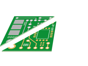
This is the process of cutting the manufacturing panels into specific sizes and shapes based upon the customer design as defined within the Gerber data. There are 3 main options available when providing the array or selling panel – scoring, routing or punching. All dimensions are measured against the customer supplied drawing to ensure the panel is dimensionally correct.
NCAB ADDED VALUE
All PCBs are profiled using NCAB approved equipment, which offers the best performance, such as positional accuracy. Default tolerances are applied to all designs if none are defined on the procurement documentation.
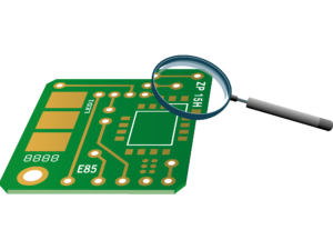
The PCBs undergo a full electrical test of the circuitry, and we visually check the PCB against acceptance criteria using NCAB approved inspectors. We also use automated visual inspection (AVI) to inspect the PCBs. AVI compares images to highlight discrepancies or concerns automatically. AVI is crucial for detecting issues in larger quantities, but the inspector’s skill remains essential for assessment. All orders are also subjected to a full inspection, including dimensional, solderability, etc.
NCAB ADDED VALUE
Each PCB is inspected against the 100+ points as defined in the NCAB product specification, and against any additional customer specifications to ensure a consistent understanding of the acceptance criteria. Every batch is subject to a full evaluation prior to shipment to ensure the PCBs are produced to the highest standard. Our onsite NCAB QC teams oversee the verification processes. NCAB does not allow track welding or open circuit repair.
Before packaging, the PCBs shall be clean and dry. Good packaging is crucial, not only to protect the circuit boards during storage at the customer’s premises, but also to ensure the solderability of the PCBs.
Both inner and outer packages should have NCAB labels. After the boards are wrapped, they are boxed prior to being shipped using the requested mode of transport.
NCAB ADDED VALUE
NCAB requires Ionic contamination level of the final PCB below 0.8μg/cm² sodium chloride equivalents for Non-HASL finishes and 1.0μg/cm² sodium chloride equivalents for HASL finishes (IPC has no requirements). Packing materials, desiccants, Humidity Indication Cards, date codes, lot codes, and the quantity of PCBs or panels per sealed pack must comply with NCAB Packaging and Labeling Instructions.
Want to know more?