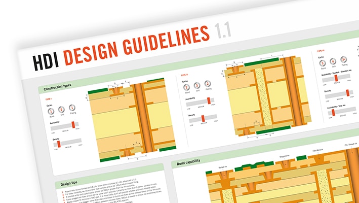
In issue no 3 of In Focus – NCAB Group´s newsletter, we dig deeper into high-tech PCBs. As an appetizer, we will already now give you some useful designtips regarding HDIs.
| COMMON DESIGN PROBLEMS REGARDING HDI | PRODUCTION PROBLEMS DEPENDING ON THIS | BEST SOLUTION |
| Dielectric too thick for laser vias | Increased time for laser drilling, lower productivity. High risk for voids in the plating process, especially in the bottom of the microvias. Increased price for the PCBs due to reduced yields. | Use an aspect ratio under 0.8:1. |
| Too small microvia size | Increased risk for the microvia to be blocked by unknown material and therefore won´t be plated satisfactorily. High risk for poor plating of the microvia, especially in the bottom. Increased price for the PCBs due to reduced yields. | Use microvias of 100 μm with an aspect ratio under 0.8:1 for microvias intended for copper filling. Use microvias of 125 μm and with an aspect ratio under 0.8:1 for microvias where copper filling is not a requirement. |
| Too tight geometries in the form of too small capture and target lands for the microvia | If the target land is too small, the risk will increase for partly missing it (so called overshoot), and material adjacent to the pad will be burnt down to the next layer. If the capture land is to small, it is a risk for the land to be broken, which is not acceptable to any class in IPC-6016. | If possible, use a start pad that is 200 μm larger than the microvia. If possible, use a stop pad that is 200 μm larger than the microvia. At tighter geometries consult NCAB. |
| Too tight demands on permitted dimple on copper filled microvias | Increased price for the PCBs due to reduced yields. | Place the requirement of dimple to a maximum of 25 μm. |

Design guidelines for HDI
Download our PCB design guidelines for HDI to get your design right from start.
