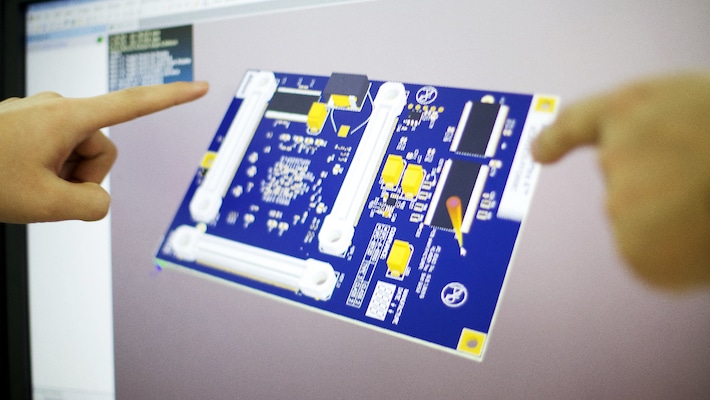
Via Hole Design – a cautionary tale
Imagine you are a start-up company. You spent a year designing a product from start to finish. You have built the prototypes; there were some snags along the way but ultimately, the end product is perfect. You’re finally ready for volume production. Once you use multiple suppliers pricing out your bare board, you discover there’s […]

More design tips – get it right from the start
COMMON DESIGN PROBLEMS REGARDING HDI PRODUCTION PROBLEMS DEPENDING ON THIS BEST SOLUTION Too tight demands on the thickness of overplating of plugged vias. (POFV or VIPPO) Affects the flow of the process, at a reasonable thickness of the overplating all the vias can be drilled in the same operation, which makes the process much […]
High-tech PCBs – design tips to get it right from the start
In issue no 3 of In Focus – NCAB Group´s newsletter, we dig deeper into high-tech PCBs. As an appetizer, we will already now give you some useful designtips regarding HDIs. COMMON DESIGN PROBLEMS REGARDING HDI PRODUCTION PROBLEMS DEPENDING ON THIS BEST SOLUTION Dielectric too thick for laser vias Increased time for laser drilling, lower […]
PCB design tips: Via-in-pad
The benefits of via-in-pad designs are well documented. From reduction of inductance to increased density, via-in-pad has become an essential tool for designers when navigating the routing challenges of fine pitch array packages that have become mainstays in today’s BOMs but there are trade-offs that must be considered. The basic concept is elegant. The via-in-pad […]

PCB DfM – a pathway to lower overall cost
It’s all about connections, not simply those that the designers make to define the circuit or the ones that circuit board manufacturers create to fab the PCB. It’s about connecting the design intent with PCB manufacturing capabilities and assembly requirements. Without these connections, the PCBA will not have the manufacturing robustness or process yield needed […]
