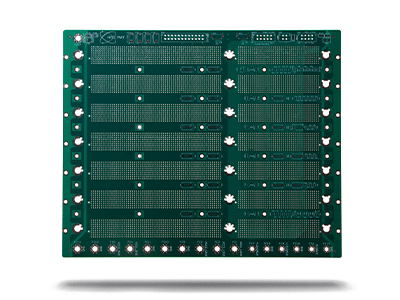
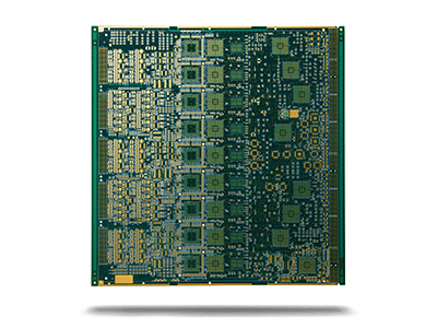
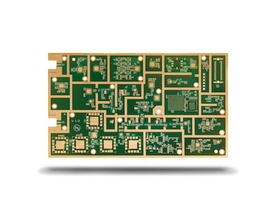
RF PCBs – Radio Frequency PCBs
NCAB works close with your product design team to insure that the project’s cost/performance targets can be met by providing information on material options, relative costs and DFM considerations.


When producing radio frequency PCBs it is important to think about how to control the signals using (i) materials types and material characteristics (loss tangent / Df and dielectric constant / Dk) (ii) low profile copper foils (iii) weave styles and (iv) how we layout the copper circuitry, as all of these factories have a significant impact on the the performance of the finished product.
Please contact your local NCAB Group company if you need further information or assistance, we are happy to help you.
Our technical capability for RF PCBs
For information about our technical capabilities for RF PCBs, read more at our Technical Capability page. You will also find information relating to materials, other PCB technologies or product types which we currently produce, as well as some of the tolerances which we can achieve.
