| COMMON DESIGN PROBLEMS REGARDING HDI | PRODUCTION PROBLEMS DEPENDING ON THIS | BEST SOLUTION |
| Too tight demands on the thickness of overplating of plugged vias. (POFV or VIPPO) | Affects the flow of the process, at a reasonable thickness of the overplating all the vias can be drilled in the same operation, which makes the process much easier. If the overplating is too thick this will reduce the possibilities to produce outer layers with thin tracks/small isolation.
| Set the requirements according to IPC-6012 class II and demand only ≥ 6 μm as overplating thickness. |
| Epoxy via plugging demands for too many different sizes of vias, this applies to both buried as for through vias | Hard to control that bubbles don´t occur in the final plug, and that there won´t be a problem with complete filling. | Only one size of the plugged vias are preferred, if more sizes have to be plugged, keep them within a range of 0.15mm. |
| Microvia placement | If microvias are placed directly into SMD surfaces, unnecessarily voids can arise in the solder joints at reflow soldering. The price structure increases if the micro vias are copperfilled. | Pull the microvias from the SMD surfaces if possible. If there is no place to do alternative 1, place the microvias right into the pad and demand for them to be copperfilled.
|
| Too small distance between the staggered holes and the microvias – microvias or microvias – buried vias | If the staggered microvias are placed too close to each other, there is a risk that the overlaying hole can intrude on the underlying one with bad plating as a consequence.This can be solved by copper filling of underlying microvias or overplating if buried vias, all this means increased cost and risk. | Regarding microvia-microvia, keep a distance of 0.30 mm between holes if possible, if not, go down to 0.25 mm. Example: 0,10 mm microvia and 0,25 mm buried hole gives 0,475 mm and 0.425mm in center to center distance.
|
Don´t hesitate to contact your local office or contact person if you have a design problem that you need help with.

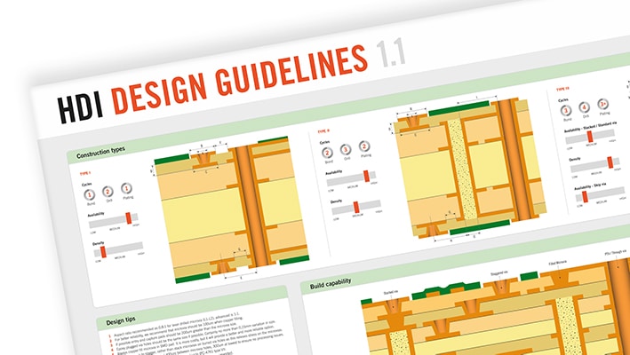
Design guidelines for HDI
Download our PCB design guidelines for HDI to get your design right from start.
