One of the aspects that generates the most uncertainty for electronics designers is defining stackups. Besides selecting the base material depending on the circuit’s application, the truth is that it’s somewhat mysterious how stackups should be managed – why thicknesses always differ from what was initially planned compared to what the factory reports after manufacturing, how and how many layers of prepregs are needed to achieve the proper insulation thicknesses, etc.
In fact, there is no instruction manual that answers every question in alphabetical order, so in this blog post, we aim to shed some light on these topics.
The typical workflow for a PCB designer is as follows:
- Select the base material(s).
- Decide the number of layers and their copper thicknesses.
- Design the stackup
Unless these variables are well-defined and agreed upon with the manufacturer, the designer cannot accurately draw traces in their CAD program.
Choosing the base material
The insulating material technology to be used is determined by the application: for an industrial circuit without high-frequency signals, we select an FR4 substrate made of epoxy resin reinforced with a fiberglass weave. In contrast, telecommunications applications operating above 5 GHz use high-frequency substrates with different fiberglass and a different epoxy resin system, which can cost up to 15 times more than standard FR4.
In high-volume commercial applications, FR4 material is used. Here, the value of the dielectric constant (Dk) or loss factor (Df) is not as critical compared to RF or high-speed data circuits.
Fiberglass weave patterns
FR4 materials are built with different fiberglass weave patterns. These woven fabrics provide flexibility to the resin base and allow thickness adjustment. The example in the below image shows the interwoven fibers of a 2114 core (center), its two copper foils (gray), together with two layers of 106 prepreg above and below. You can see that the thickness difference is mainly achieved by using different fiber sizes.

Fiberglass-reinforced resin substrates have evolved over time to offer improved thermal, electrical, and mechanical performance: lower Z-axis CTE, lower X-Y CTE, greater crack resistance, and a wide variety of resin options not possible with other materials. These features, along with their affordability, make them the most widely used base materials in the PCB industry today.
When we reach the realm of high frequencies and high-speed data, we encounter the limitations of FR4 materials:
- Dielectric constants (Dk) must be stable over a wide range of frequency and temperature, and it is usually preferable to have low Dk values to reduce signal delay and facilitate controlled-impedance routing.
- Low dielectric loss (low Df) is also required to control the loss of signal energy.
- Likewise, thermal demands on the substrate are higher due to the environments in which these PCBs are typically used.
Unlike FR-4 materials, whose manufacturing processes are highly standardized and result in high yields at competitive prices, the opposite is true for some high-frequency laminates:
PTFE (Teflon) laminates offer excellent electrical performance but typically require factory processes that often fall outside standard manufacturing practice. This makes them significantly more expensive and can even make fabrication unfeasible when these processes differ from those used for FR4 materials. In these cases, everything depends on the technical capabilities of the factory.
To address this problem, materials with optimal electrical properties that can be processed using methods similar to FR-4 have been developed. This is the origin of ceramic-filled PTFE substrates and thermoset hydrocarbon laminates. Both maintain very good electrical characteristics and present fewer manufacturing challenges.
Deciding the number of layers and copper thicknesses
A lot of factors must be considered here. As in construction, when the available area is small, you build upward. In a PCB, the final area tends to approach the surface occupied by the component footprints. In some cases, we are preparing to challenge this limit: IPC-7092 defines the processes needed to embed active and passive components within substrates, but here we will stick to standard PCB manufacturing technologies.
Discrete components continue to optimize their packaging: BGA formats now reach below 0.4 mm. Routing such a concentration of pins per square centimeter requires a large number of layers, and if pitch reach 0.35 mm or below, we even need new manufacturing technologies such as mSAP.
Controlled impedance lines and heat generation
Another determining factor in PCB layer count is whether controlled impedance transmission lines are required. Controlled impedance lines need reference planes either below (microstrip topology) or above and below the controlled impedance lines (strip line) and therefore increase the number of layers. These lines also determine the thickness of the insulating layers (impedance and prepreg thickness are directly related).
Finally, another factor influencing PCB topology is heat generation: copper is not a perfect electrical conductor and generates losses in the form of heat that needs to be dissipated. The different currents flowing through power nets determine the thickness of power planes. In such cases, it is the PCB designer who specifies the thickness to be used from the wide variety of available copper weights.
To protect the PCB against excessive temperature, the optimal measure is to ensure that under normal working conditions the temperature rise does not exceed a safety margin below the material’s Tg. For this, we rely on the IPC-2152 charts.
Designing the stackup
Once the material technology and number of layers have been determined, the total nominal thickness must be adjusted. Although 1.6 mm is the most common, any other thickness can be specified if needed.
The most common manufacturing process is based on stacking laminated cores alternately with prepreg layers (which also provide the resin needed to bond and laminate the stack). The stack is completed externally with two copper foils bonded to the assembly using prepreg. This stacking order is what we know as the stackup.
As a design rule, for a conventional circuit (non-HDI), the two outer insulating layers in a PCB are always prepregs because they serve as support for the top and bottom copper foils. The remaining internal layers are built from laminated cores also bonded with prepregs. The result is a distribution that always yields an even number of layers.

Download our design guidelines for Stackups and impedances
Maximum three prepreg layers
Prepreg layers can be combined to achieve the desired insulation thickness between layers, but no more than three layers may be used at the same interface. When the required thickness between two copper layers is so great that it cannot be achieved with three prepregs, an additional copper-less laminated core is used. Copper-less laminates exist, or some factories remove one or both copper layers by etching.
The correctly stacked and aligned assembly is placed in a vacuum assisted hot hydraulic press at about 175°C (around 30 °C above the material Tg) and 3000 kg/sqm of pressure for about two hours until the assembly cures and becomes a single block.
This is where prepreg thickness reduction occurs, often surprising designers: the resin flows into the gaps left in the copper layers after etching the traces. This reduction is usually not considered when planning nominal layer thickness.
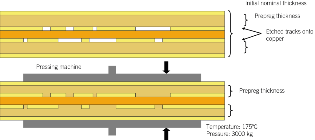
One interesting effect of this prepreg thinning is that the characteristic impedance of signal traces decreases, as the reference planes are now closer to them.
At this point, calculations must be adjusted. For this, the datasheets of the prepreg and core manufacturers are needed, as well as details of the etched circuit, specifically:
- The nominal copper thicknesses.
- How much copper is used in each etched layer – that is, the percentage of copper remaining after removing areas that are not traces, planes or pads. The percentage of copper removed corresponds to the volume occupied by the adjacent prepreg when its resin melts.
- The nominal thickness of the prepregs used.
Calculation process step by step
Returning to our initial problem: what is the resulting thickness, and how are these compensations made? Let us detail the calculation process step by step:
- Define the initial thicknesses of each layer based on design criteria:
– Laminated cores usually specify thickness including copper (depending on manufacturer). In these cases, the true insulating thickness is obtained by subtracting the two copper foils; to know this exactly, the manufacturer’s specifications must be checked.
– Choose the initial prepreg thickness for each insulating “ply” according to the chosen configuration—for example, the thickness required to achieve controlled impedance.
– In most cases, thicknesses are adjusted simply to achieve the total 1.6 mm. - For each copper layer, calculate the percentage of copper removed during etching.
- Calculate the compensation applied by the prepregs adjacent to each copper layer.
At NCAB, we assist with these calculations and coordinate with the factory to obtain the most accurate and realistic adjustments possible. - Verify that the prepreg compression margin does not exceed recommended limits, meaning that the fiberglass weave inside it is not excessively compressed. Maximum compression limits are provided by the material manufacturer and applied precisely by the PCB fabricator.
The following table shows an example that illustrates each of the key points discussed in this section. Remember that adjustment margins depend on the specific PCB manufacturer.
The “Final Thickness” column shows the theoretical resulting thicknesses.
We must also consider another important manufacturing aspect: the reduction in thickness resulting from cleaning, drying, polishing, etc., of copper foils. These limits are specified in IPC-6012, table 3-18 for external copper layers and table 3-17 for internal copper layers but can also vary between factories and manufacturing methods used.
Conclusion
We hope the stackup adjustment methodology presented here provides clarity for designers who do not have automatic thickness-calculation tools, and we reiterate the need to involve the manufacturer in this process, as they are the ones who know the practical behavior of the materials they work with and how much their own process affect the final thickness of both copper and prepreg material.
We can support you in defining the stackup for your new designs, helping you create a design adapted to manufacturing processes, avoiding issues during production, and ensuring scalability to mass production if needed. You can reach out to your local NCAB Group contact for any PCB-related inquiries – we will be happy to assist you.
Download our design guidelines for Stackups and impedances
We also have design guidelines for Multilayer PCB, HDI PCB, Ultra HDI PCB, Flex / Rigid-Flex PCBs, Semi-Flex PCB, Copper coin and Via Protection – all to help you get your design right from start!