Printed circuit boards (PCBs) can have various surface treatments, including electroless nickel/gold, HASL, immersion tin, and OSP (Organic Solderability Preservative). But what is the purpose of these finishes? Their primary role is to protect exposed copper, ensuring it remains intact during storage and is ready for soldering (SMT, wave soldering, selective wave, manual soldering, etc.).
Soldering and surface finishes
During soldering, the surface finish dissolves in solder paste or tin (wave soldering), and the solder joint is formed with the copper. However, in the case of an electroless nickel/gold finish, the protective gold layer dissolves in the solder, and the joint forms with the nickel instead.
PCB surface treatments can be categorized as organic or metallic, each with distinct advantages and disadvantages. The choice of finish depends on the end application, assembly process, and PCB design. Among these finishes, one stands out for its exceptional durability: the hard gold finish. This blog post explores what makes hard gold unique and its most common applications.
What is a Hard Gold Finish?
A hard gold finish, also known as electrolytic hard gold, is an electroplated gold layer that is thicker and more durable than other finishes like ENIG (Electroless Nickel Immersion Gold). It is alloyed with metals such as nickel or cobalt to enhance hardness and wear resistance, making it ideal for high-contact areas that require long-lasting electrical connections.
Due to its durability, hard gold is applied to PCB regions subject to frequent mechanical stress. Common applications include edge connectors and keyboard contacts, all of which require robust, high-wear connections for data transmission and electrical continuity.
Applications of Hard Gold Finish
Edge Connectors (Gold fingers):
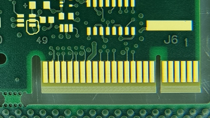
Edge connectors, often called Gold fingers, are one of the primary applications of a hard gold finish. These electrolytic nickel/gold-coated copper fingers or pads are located along the edges of PCBs, serving as critical connectors for electronic modules. They play a key role in ensuring seamless data transmission between interconnected components in devices such as computers, smartphones, and industrial equipment.
A hard gold finish is essential for edge connectors, ensuring reliable and durable connections between PCBs and external components. The enhanced hardness and wear resistance of the gold alloy allow these connectors to maintain strong electrical connections over extended periods, even with frequent use. Edge connectors are particularly used on PCI (Peripheral Component Interconnect) boards, which require repeated insertions and removals. The thick, hard gold layer enhances resistance to mechanical wear, making it an optimal choice for high-use connections.
Examples of Hard Gold applications:
- RAM Modules: Gold Fingers ensure a reliable connection between the memory modules and the motherboard.
- SIM Card Connectors: Used in smartphones to ensure a stable and long-lasting connection between the SIM card and the phone.
- Server Expansion Cards: Allows you to add additional storage or network capacity to servers.
- Industrial Motherboards: Withstand a variety of harsh environments and working conditions.
Keyboards and Key Contacts – Selective Hard Gold:
Keyboards or key contacts are prime examples of selective hard gold plating, where the finish is applied only to specific high-use areas. In keyboards, gold plating is used on key contacts to ensure longevity and consistent performance. The gold layer prevents wear and degradation, maintaining reliable electrical connections despite repeated keystrokes. These contact areas inside the PCB need what we call selective plating. Even with selective plating, every area that is to be plated needs to be electrically connected outside the PCB area, similar to the tie bards we use for edge connectors. These connections can be designed in the top or bottom layers, but very often, inner layers are used for such connections. This requires good planning in the PCB design stage, and we strongly recommend seeking help from your local NCAB Field Application Engineer.
Technical specifications for Hard Gold finishes:
| IPC Class 1 | IPC Class 2 | IPC Class 3 | |
| Minimum Gold Thickness | 0.8µm | 0.8µm | 1.25µm |
| Minimum Nickel Thickness | 2µm | 2.5µm | 2.5µm |
NCAB default requirement is IPC class 2. In comparison, for the ENIG finish, the minimum electroless gold thickness is 0.05µm.
Advantages
- Durable finish, resistant to mechanical friction.
- Long service life.
- RoHS compliant.
Disadvantages
- Expensive.
- Not intended for soldering.
- Can conflict with other solderable finishes on the same board. (Ask your local NCAB FAE for advice.)
- Selective Hard Gold needs a suitable design for plating connections.
Manufacturing process
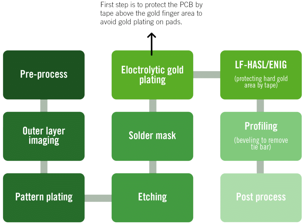
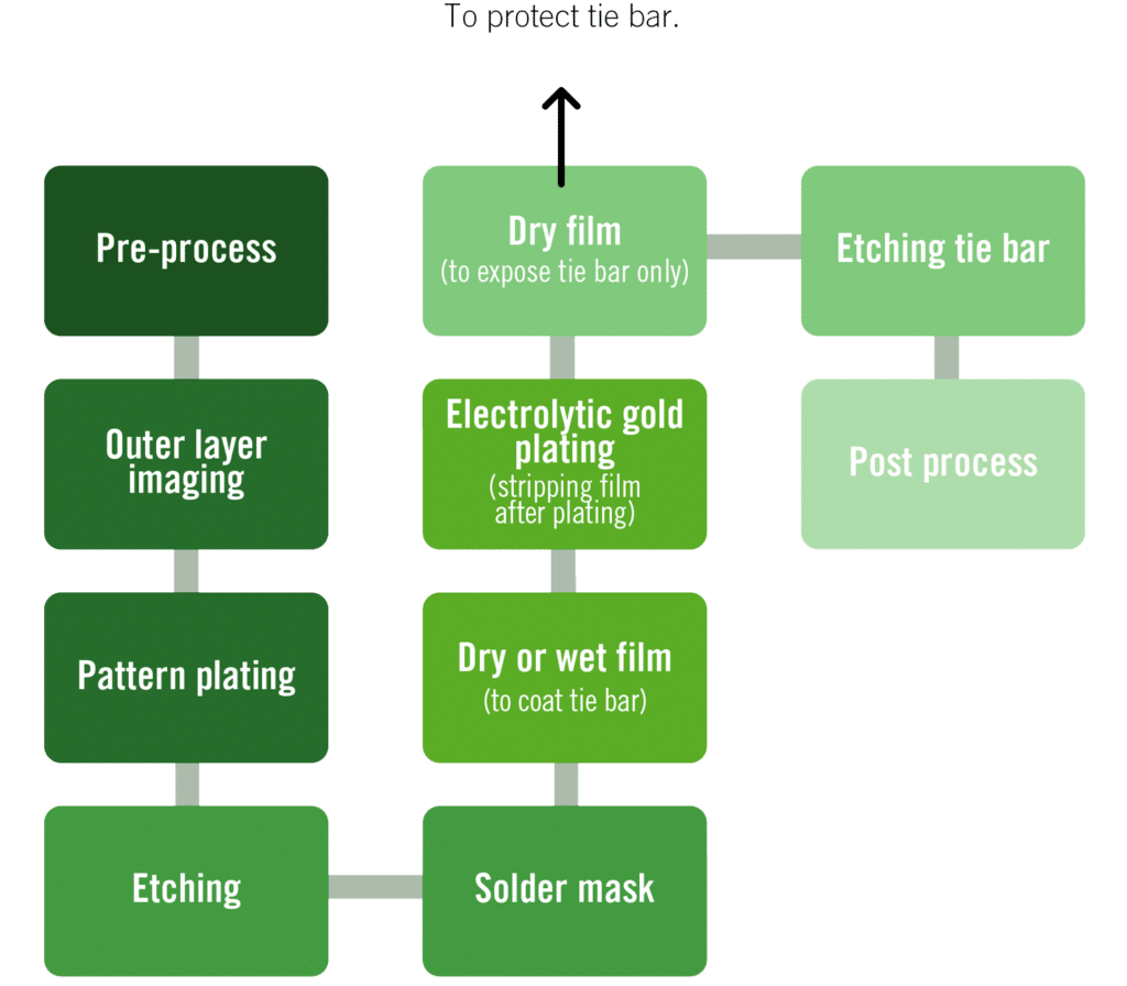
Since a hard gold finish is applied through an electrolytic process, additional copper tracks are needed to connect the gold-plated pads to the anode. These tracks must be removed after plating, which can be done in two ways:
1. Mechanical removal by chamfer
2. Removal by etching
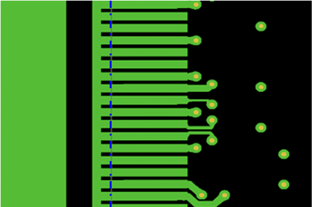
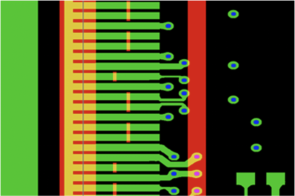
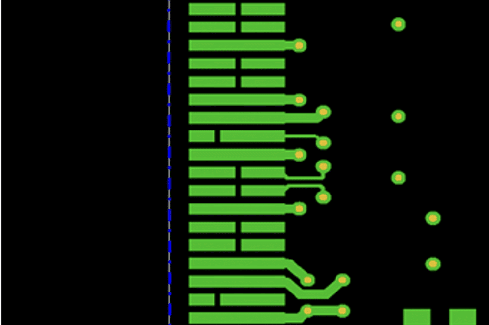
This also explains why hard gold keypads with selective plating need good planning in the design stage.
Conclusion
A hard gold finish is the ideal choice for PCBs that require long-lasting, high-wear connections. While it is more expensive due to its increased gold thickness, it offers superior resistance to mechanical friction and ensures a long service life while remaining RoHS-compliant. For a detailed cost estimate or further information, please contact your usual NCAB contact.
