Heavy copper PCBs

What is a heavy copper PCB?
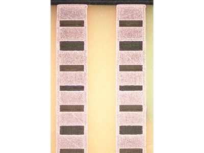
It is a PCB made with two or more conductive copper layers. The conductive foil appears to be thicker than on standard PCBs. The different inner layers are processed in pairs (on a core) and then bonded together using prepreg as the insulating layer. The layers are then placed in such a way that both sides of the PCB can be used to mount components with additional tracking/electrical connections on the inside of the board. Vias are used as a source of the electrical connections between the different layers of the PCB.
More and more products are using heavy copper PCBs, for example EV-chargers, high current systems and power storage systems.
Please contact your local NCAB Group company if you need further information or assistance, we are happy to help you.

Download our PCB design guidelines
Use our design guidelines to get your PCB design right from the start.

Contact us
Please contact your local NCAB Group company if you need further information or assistance, we are happy to help you.
