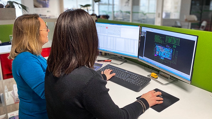
More than 30% of the data packs we receive contain elements or features that needs clarification. And if a prolonged EQ (engineering questions) process is to occur, then it is highly probable that your PCB’s total cost and reliability can be negatively impacted. Therefore, it is important that our technicians and customers work systematically to clarify any uncertainties from the very start.
So, how can we do this? In order to complete the EQ process faster and to ensure that the end product is reliable, an efficient engineering process needs to be put in place. From the Gerber files to the various features and elements of the PCB which are to be documented, our technicians help to ensure that each of these aspects are dealt with early on.

What is in the Gerber files?
The Gerber file format is the standard used to transmit information about the printed circuit board manufacture. It includes the description (tracks, pads, CMD pads, vias, etc.). Gerber RS-274X (Gerber Extended) is the standard format for PCB design software. It is used to manufacture about 90% of the PCBs which are currently produced in the world.
At NCAB Group, we are also able to load files in ODB++ format. This is a smart format that contains all the information needed to produce a PCB, and limits the risks when used by CAM departments to generate producing tooling.
Gerber RS-274X or ODB++ format, the files must include the following:
- All the layers (top / bottom layers, inner layers)
- Top and bottom soldermask
- Top and bottom silkscreen (if existing)
- Routing file
- Netlist provided under IPC-D-356 format
Contrary to popular belief, Gerber data does not include drilling files. These files are very important because they gather the drilling specifications of the PCB: plated through holes (PTH), non-plated through holes (NPTH), slots, microvias sequences, buried vias, counterbores, specific tolerances, etc.

Key features and elements of the PCB to consider
In addition to the Gerber files (or ODB++) and the drilling files, it is essential to attach a master drawing indicating the key requirements of the PCB. This in turn will not only indicate your required specifications for your PCB but will also reduce the time to market. The requirements which are to be documented and communicated to the technicians are the following:
- Project stage – Is it a prototype, a pre-series, a series, or initial samples? This information helps us to select the most suitable plan from the start to meet your needs.
- Technology – A printed circuit board can be simple-sided, double-sided, multilayer, HDI, flex, rigid-flex, semi-flexible or IMS.
- Standards & application – Specify the application for which the PCB is dedicated for. This allows us to quote according to the required standard and to better respond to your request.
- Material according to IPC-4101 – We recommend specifying the IPC grade (IPC-4101/99, 101, etc.) which defines in detail the characteristics of the base material, or the Tg (FR4 Tg 130°C, 150°C or 170°C).
- PCB size – In addition to the dimensions of the PCB, it is advisable to specify the desired delivery format: single PCB, PCB with technical edges, panel drawing
- Panel drawing – Each customer has their own rules in terms of panel drawing (size, technical edges, test patterns, etc.), which is why we invite you to communicate them to us as well as the cutting method (V-cut or stamps holes).
- Surface treatment – The decisive factors in choosing the most suitable finish are the design of the PCB, the assembly process, the final application, and the storage time.
- PCB thickness – The standard thickness of a rigid printed circuit is 1.6mm but depending on the technology and the number of layers, it can vary from 0.05mm to 8mm.
- Internal/external base copper thicknesses – The standard thicknesses of the copper layers are 17µm, 35µm and 70µm. Beyond these thicknesses, there may be a material lead time. Regarding the outer layers, it is important to specify whether it is the base or finished copper thickness.
- Soldermask – The soldermask can be mat or glossy. It is traditionally green but there are also many other colors (black, blue, red, yellow, white, etc.).
- IPC class acceptation – At NCAB Group, our printed circuit boards are produced according to IPC Class 2 except if the customer requires IPC Class 3.
- Mechanical drawing – It’s important to mention the hole size, tolerances, and types: PTH, NPTH, press-fit, slot, etc.
Along with our efficient engineering process, and our clients becoming more familiar with the required documentations and components which are needed to be communicated early on into the process – Gerber files, drilling files, key requirements – we can ensure that your PCBs are made with zero defects and within a cost-effective production. Our technicians have many years of experience within PCB production, specifically about how to produce PCBs without compromising your design goals. Therefore, if you have any questions or want to reach out, then please contact the respective local office or contact person.
What other PCB cost drivers are there?
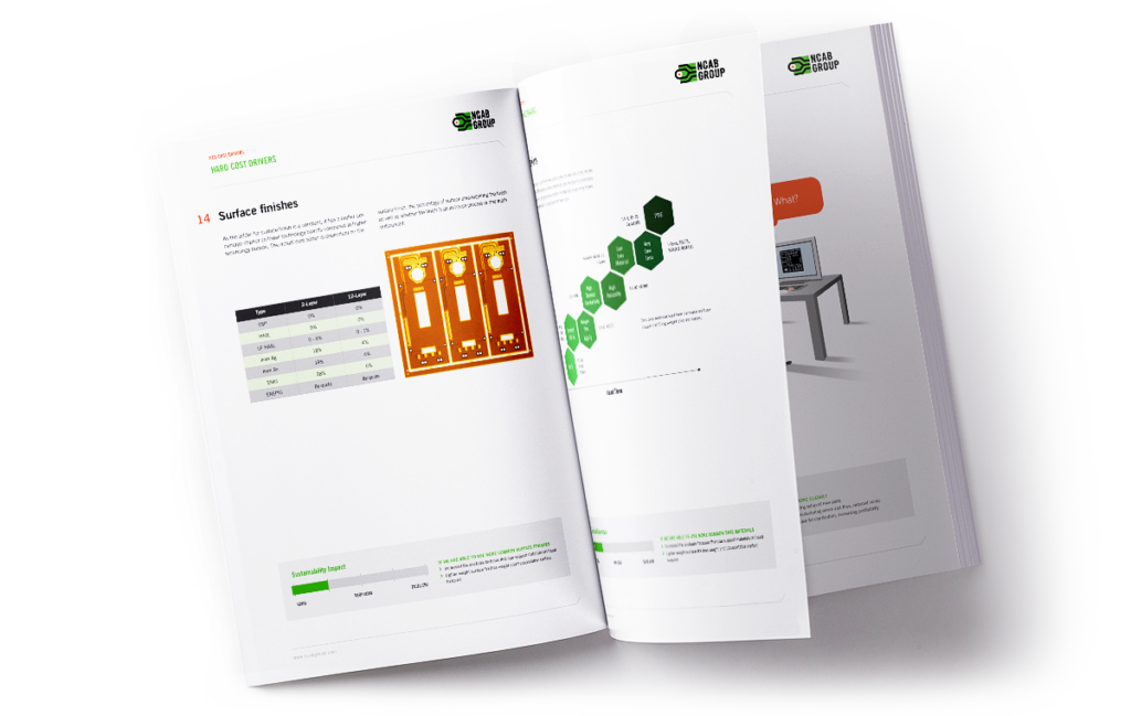
Download our free tool PCB Cost drivers and learn about how you can decrease the cost of your PCBs, and in the same way get a more sustainable product.

