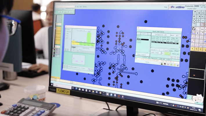
Fabrication notes, Drill Table, Scaled Drawing, Stackup Drawing and Array Drawing are all parts of a PCB fabrication drawing. But – what is a fabrication drawing – and why do you need it? This blog post will tell you all you need to know about this topic, and give you examples of best practices.
Unlike the components that are soldered to PCBs, circuit boards are custom manufactured goods that take time to design and build. The more complex a PCB is, the more fabrication documentation is required. Regardless of the PCB’s complexity, a fabrication drawing will speed up the manufacturing process by answering many questions a PCB supplier would have. The supplier will use the fabrication drawing in conjunction with the PCB manufacturing data for verification.

Fabrication Drawing – The Purpose
The purpose of the fabrication drawing is simple: it serves as a blueprint for the PCB. There is no “one size fits all” solution to building a PCB, as each board has unique manufacturing and quality requirements. These must be specified by the user. The fabrication drawing is also used for verification, as CAD systems sometimes generate bad data, which is often unknown until the Design for Manufacture analysis at the factory. Additionally, the fabrication drawing is used for qualification, allowing quality personnel to ensure the PCBs meet all IPC specifications during final inspection.
Fabrication Notes
The fabrication notes serve as a tool for PCB design engineers to specify the fit, form, and function of the final product. In addition, the fabrication notes are communication between the PCB designer and fabricator. Engineers can also use the fabrication notes to control the quality of the PCB. This section of the PCB fabrication drawing should provide accurate specifications for the finished PCB. In order to maximize the effectiveness of the fabrication notes, a PCB design engineer should be familiar with the IPC specifications. The Qualification and Performance Specification for Rigid Printed Boards, IPC-6012, provides design engineers many options to specify on the finished PCB.
Specify a quality class of the PCB
For example, when specifying the surface finish, engineers can also specify the durability of the surface finish. This is vital to ensure the PCB can withstand storage and the amount of heat cycles necessary for assembly. This example also illustrates how the IPC specifications are used in conjunction with each other as IPC-6012 refers to the Joint Industry Standard -003 (J-STD-003). Another way to control quality, and cost, is to specify a quality class of the PCB. For example, IPC-6012 Class 3 may be required for a high reliability PCB, whereas Class 1 and 2 will have less quality requirements and inspection points. Moreover, Class 1 and Class 2 will also demand lower overall cost. It is common in the PCB industry to see circuit boards specified to meet the Class 2 manufacturing requirements, but manufactured with some Class 3 requirements, like plating.
A great way to specify base materials is to look at the base material specifications from IPC. IPC-4101 and IPC-4202 use “slash sheet numbers” to identify and categorize PCB materials based on material grade.
It is very important for the notes to be written as simple and as clearly as possible. Vague or open-to-interpretation notes can lead to manufacturing delays or errors, resulting in unnecessary costs and lost time.

Drill Table
The drill table is another element of the fabrication drawing used for design verification. It lists all the holes to be drilled into the PCB, including their sizes, quantities, tolerances, and symbols that match the drill drawing artwork. These symbols indicate the placement of each hole on the PCB. PCB designers can also add extra information, such as for blind and buried vias, to minimize questions. Sometimes CAD systems generate mistakes that are out of our control or unknown to us, so spending extra time on this area provides additional assurance.
Scaled Drawing
Part of the fabrication drawing should be reserved for a scaled PCB outline drawing. This drawing should provide an accurate outline for the PCB. . I know what you are thinking… A simple scaled PCB outline will work for many designs, but to make the best fabrication drawing possible, more details are needed. In addition to the outline, scaled dimension lines should be added, and a good drawing will include an origin point for the manufacturer to reference.
In my factory days, I learned to always check the scaling first. Often, the customer’s CAD system was incorrectly configured for Gerber data output, causing the physical layers to be scaled differently than the drill files. When the PCB dimensions were included, I could figure out the issue rather quickly. Although this is a small reference to add, it is useful.
However, adding too many dimension lines can crowd the drawing and make it unreadable. I recall a circular board drawing with so many dimensions and angles that our engineers couldn’t understand it. It’s best to include only overall and critical dimensions.
Stackup Drawing
A stackup drawing (or simply “stackup”) is a detailed cross-section image of the PCB. While not always needed in every PCB design package, some designs require specific information. For a two-layer PCB, a designer can list the finished board thickness and tolerance in the fabrication notes. However, some designs will need a stackup drawing with specific details.
PCB designers can specify the layer arrangement, but in my experience, some PCB design packages fail to be this simple.
PCB designers can specify finished copper thicknesses for each layer. This is great information as long as it’s accurate. However, I have seen stackups that specify copper thicknesses for internal layers that did not match standard manufacturing thicknesses. This is acceptable if it’s mutually agreed upon between the user and supplier (AABUS). Listing non-standard copper thicknesses without reasoning can generate questions and place the board on hold in engineering, as non-standard manufacturing will likely add more lead time and cost to the PCB.
Include material type in the stackup drawing
PCB designs with blind, buried, and/or back drilled vias can have complex drill sequences. A drawing showing all the drill sequences will inform the PCB supplier about the number of press and drill cycles before final inspection, eliminating the need for guesswork. While a supplier can determine each segment from the PCB artwork, an educated guess is still a guess.
The stackup should also include the material type and finished dielectric thickness of the PCB materials. This information is usually only necessary for PCBs with controlled impedance requirements. The material type and dielectric thickness help control impedance traces, and with careful planning, engineers can minimize Electromagnetic Interference (EMI) and crosstalk through strategic reference plane placement.
The stackup drawing is a great way to document Controlled Impedance specifications. The best impedance trace callouts are placed in a table, identifying the impedance traces on every layer. The table should also include trace width, space for structures, target impedance value, and the layers each trace will reference.
Some PCBs have thermal management specifications like Insulated Metal Substrate (IMS) or Copper Coin Technology. Copper coins and metal substrates come in various shapes and sizes. The stackup drawing is a good way to show the thickness and shape of the coins and the details of the IMS technology, such as thermal dielectric and metal substrate thickness.
What is controlled impedance?
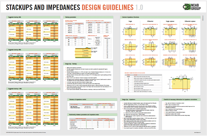
NCAB’s detailed stackup drawings specify layer arrangements, copper thicknesses, and drill sequences, ensuring that the PCBs meet controlled impedance requirements. Learn more about controlled impedance and download our PCB design guidelines for Stackups and Impedances to get your design right from the start.

Design guidelines for stackups and impedances
Download our PCB design guidelines for Stackups and Impedances to get your design right from start.
Array Drawing
The array drawing is a scaled drawing illustrating the number of circuit boards in each array. It should depict dimension measurements and have accurate spacing between each PCB. The rails of an array should have at least three fiducials used by factory machines to maintain accuracy through assembly. If thieving is needed to ensure more uniform plating across the panel, the rails are a good place to add it without affecting the circuit board.
The array helps with cost and quality control. Processing all PCBs in an array ensures consistency throughout the lot and is more cost-efficient than handling single units. Optimizing the array to minimize waste material can drive costs down, but be cautious: too many PCBs on a single array or removing too much waste material can make the array unstable and cause it to fall apart before assembly. Optimizing the array for efficient assembly can reduce costs and waste. If you lack this skill, don’t worry.

What drives the cost of a circuit board?
Speaking of being cost efficient & driving costs, NCAB emphasizes designing PCBs in a cost-effective manner without compromising on quality. For instance, by designing less complex boards, we can reduce production time, labor, and material costs. Download our PCB Cost Drivers to see how you can avoid large costs.
Sooner or later, the circuit board may need revisions. An updated fabrication drawing will reduce front-end engineering time. Many engineers and buyers complain about the time a PCB spends in front-end engineering. This gives the customer more control during this time. Besides updating the fabrication drawing, be cautious when specifying redundant information across several sheets. Greater redundancy increases the risk of missing something during revision, leading to additional questions and longer lead times.
It’s a great feeling when the PCB fabrication drawing is complete. The drawings should be clear and concise while containing all pertinent information. If details distract from the meaning of the note or drawing, it may be better to revise it. Circuit boards are custom designs. The PCB supplier knows how to manufacture PCBs, but they may not have manufactured your particular design. This will require some questions, but the goal of the PCB fabrication drawing is to minimize these questions. Optimizing this part of the design is time-consuming, but it is worth it for better quality, cost, and lead times.
