As technology continues to advance at an exponential rate, thermal management is becoming an ever increasing issue at the bare PCB and assembly level. Whether it is high brightness LED applications, high power transmitters or a high voltage power supply, the demand for better heat transfer and cooling is also increasing.

The overall goal of thermal management at the bare board and assembly level is to move the heat away from the heat-generating components to an external heat sink for dissipation. Better heat transfer will usually translate to lower mean time between failures (MTBF) and at times will be a deciding factor at meeting product design specifications.
MCPCB technology
A simple way to manage heat is switching from FR4, the standard material used in multilayer PCBs, to utilize different thermally conductive dielectric materials bonded to a solid sheet of base metal, metal core (MCPCB). This will significantly increase the thermal performance of a PCB. MCPCBs works by utilizing a thermally conductive prepreg between the copper routing layers which draws the thermals down to the metal core or base and away from the componentry. MCPCB technology can be accomplished as a single layer over a metallic base or as a multilayer on the top and bottom sides of the metallic base.
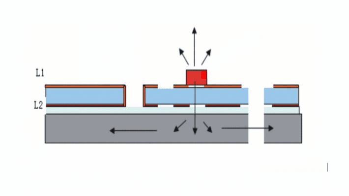
Below is a 2 layer MCPCB construction that shows the transfer of heat from the surface mount component through the buildup to the base metal. This can offer thermal conductivity of up to 12 W/mK but at present this solution cannot offer any better results than this. For a higher thermal conductivity an alternate technology such as copper pedestal or copper coin is our recommended solution.
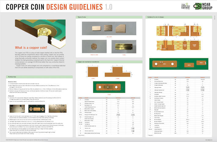
Design guidelines for copper coin
Download our PCB design guidelines for Copper Coin to get your design right from start.
The growing technology of copper coin PCBs
For this article we want to dive deeper into the growing technology of Copper Coin PCBs. Heat transfer occurs at a higher rate when materials of high thermal conductivity are used. Copper is extremely conductive offering upwards of 400 W/mK, as is for example other materials like diamonds, which can be up to five times more thermal conductive than copper. But, who wants to use diamonds in their PCBs? Copper is one of the best ways to manage heat while keeping electrical and or thermal conductivity.
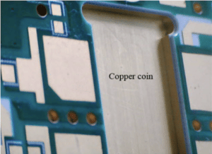
The copper coin PCB is simply a piece of solid copper inserted onto or into the PCB, typically under the component(s) which need cooling. Copper coin can provide about twice the cooling compared to a via farm. And instead of using thermally conductive material, the copper coin can provide direct contact between the heat-generating component pad to the heat sink. Copper’s thermal conduciveness is on average 30-200 times better than any conductive dielectric prepreg out there.
When is copper coin best to use?
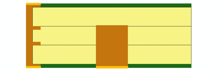
Copper coin technology is best suited when there is a specific or a small number of components on a PCB that are responsible for most of the heat generated. Copper coin is providing the ultimate heat transfer solution in a localized fashion on a PCB regardless of the number of layers or the PCB material. The concept is based on getting a copper coin press fit into a premade cutout in the board right under an area that is identified as a hot spot, allowing the heat to be transferred directly to a heat sink through the PCB stack-up. This is of course without passing through the PCB buildup materials which historically have caused a thermal dissipation bottleneck.
The copper coin is inserted into the PCB and can be incorporated in different forms and configurations. The configuration chosen by the designer is reflecting the trade-off between routing, power plane requirement and proximity of the copper coin to the component that needs to be cooled.
Image examples
Image 1 and 2 shows a solid copper path from layer 1 to layer 4, acting as the assembly pad and providing the ultimate heat transfer channel for a hot component.
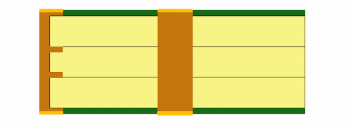
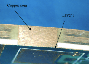
In other cases if the pad size is too small and there are routing considerations under a hot pad, the copper coin can be pressed fit only up to a designated layer and not through the entire PCB. Below we see the implementation of a copper coin (image 3 and 4) that is placed between L4 and L2 and does not make contact with L1.
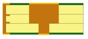
The image below shows an example of a ‘T’ shaped coin. The T shape is an example of how to use the superior properties of copper coin topology in which either the heat generating pad or the heat sink are different in their area – a small pad and a large heat sink or the other way around. Another use case is if there is a limitation to how small a copper coin can be. Using a T shape, allows us to keep the overall dimension of the copper coin within the minimum, and still create contact with a pad that is smaller than the minimum copper coin size requirement. T coins offer an excellent trade off in terms of performance and real-estate because the shape allows for flexibility with the space the coin will occupy.
While this technology is still relatively new, we have seen much success when the PCB is designed optimally for this. Any time you’re putting a foreign object into a stack-up, registration and tolerances become a big concern and there is a greater need for process control. Copper Coin is the pinnacle for thermal transfer that can be efficiently applied to at the bare PCB level. Whether you are working on a MCPCB design or a copper coin design, we recommend always working with your PCB supplier, particularly with these new technologies.
Need more information about copper coins?
Please contact your local NCAB team for guidance and support with any projects you have.
