There is a growing need for special solutions to handle excess heat in electronic products. Rapid technological developments have increased the requirements, not least with regard to PCBs. In this blog post, NCAB’s experts describe developments in this area and the methods available for thermal management.
MORE ARTICLES ON THIS TOPIC:
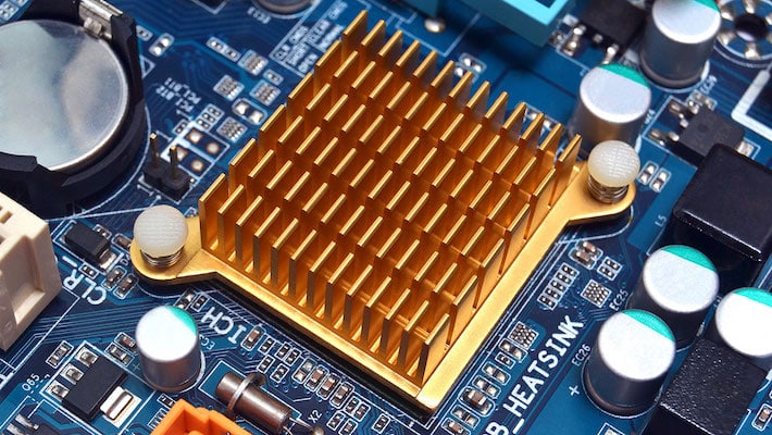
In modern electronic systems, and especially in power applications, we must always place attention on two main aspects; efficiency and thermal management. The efficiency determines how much of the power is actually transferred without losses. Thermal management seeks to ensure that the devices in the system can operate while remaining at an acceptable temperature level. Basically, thermal management refers to the methods used to transfer excess heat from one place to another. Traditionally this was accomplished by affixing an external heatsink over a particular component which generated excess heat. But what if the PCB itself was generating the heat? Or what if your component did not mechanically allow for a heatsink to be secured on top of it?
Current that is not transferred correctly is inevitably transformed into thermal energy. This thermal energy must be removed, so as not to cause an increase in the temperature of the devices. If this is not adequate it could lead to damage to the components or in any case to a reduction in their life.
In the case of electronic devices and PCBs, our goal is to transfer excess heat away from the component, dissipating heat within or across the PCB from side to side. Sometimes we do this in combination with active solutions such as ventilation through external heatsink or liquid cooling.

“You have to get creative and find new approaches to dissipate or redirect the excess heat.”
Jeffrey Beauchamp
Technical/Engineering Manager, NCAB Group USA
Innovation increases the need for thermal management
In recent years, we’ve seen a steadily growing need for thermal management solutions in electronic systems. Jeffrey Beauchamp, Technical Manager at NCAB Group USA and Mario Cianfriglia, Field Application Engineer at NCAB Group Italy, explain how this need has been driven by technical innovations in the industry.
“One of the most important trends in electronics manufacturing right now is about miniaturization, with smaller and smaller products and components as well as more compact printed circuit boards. This makes it increasingly difficult to apply traditional solutions such as heat sinks because they take up too much space. So you have to get creative and find new approaches to dissipate or redirect the excess heat.” Jeffrey Beauchamp explains.
Another new factor that designers face is managing the higher temperatures generated by new components performing more functions, calculating at higher speeds. The faster the computation speed, the hotter the components become.
”Essentially the PCBs are forced to be miniaturized, in order to use ever smaller electronic components, in which interconnections have evolved in terms of quantity x square centimetre (Cm2). This is all to accommodate the latest generation of BGA components with 0.4 mm pitch or smaller, which manage the digital and power signals,” says Mario Cianfriglia.
Thermal management of applications, a challenging task
Mario Cianfriglia also emphasizes that designers are facing new challenges since electronics are being integrated into an ever-increasing number of applications.
“In some cases, heat management can be extremely demanding, for example in the energy sector, industrial applications or the automotive industry, especially when it comes to electric vehicles. The same applies to more complex applications such as in telecommunications or radar systems,” he says. With the ongoing implementation of 5G, the fifth generation of mobile communications, electronics products will incorporate an increasing number of components running at even higher speeds and generating more excess heat. At the same time, assuring signal integrity in 5G applications will be absolutely essential.
“PCBs are currently capable of handling 3 to 5 Ghz signals, but with the full functionality of 5G they would [have to] handle signals of about 25 GHz and beyond.”
Mario Cianfriglia
Field Application Engineer, NCAB Group Italy
”This is the last frontier of technology, where signal integrity is essential. PCBs are currently capable of handling 3 to 5 Ghz signals, but with the full functionality of 5G they would [have to] handle signals of about 25 GHz and beyond. To ensure signal integrity in all operating conditions, it is very important we have the correct thermal management. PCBs with high frequency signals must be designed with an appropriate stackup, special raw materials, the routing of the traces and the ground planes, power supply and signal.” says Mario Cianfriglia
“We’re just starting to see an increase in demand for thermal management and I think it’s probably going to continue to increase. Hopefully with it come new, more advanced measures for managing the heat issues.” says Jeffrey Beauchamp.

Analysis programs prevent problems
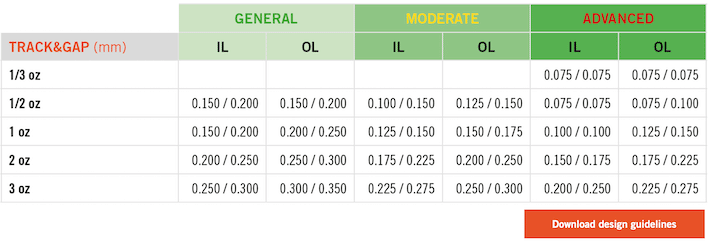
In product development, various techniques are used for identifying potential problems related to heat. Special software packages have been developed for preventive analyses. It is important that everything is correctly dimensioned in the design of printed circuit boards already at the design stage. Here you need to know the requirements of the components, size of the track and gap according to what they will have to support — in terms of signal speeds and power — and select the appropriate thickness of copper and base material.
There are also thermal analysis tools, many software packages are used for a preventive analysis, where everything can be dimensioned at the design level. It is necessary to know the needs of the components, to size track and gap according to what they must support in terms of fast signals and power, to select the right copper weight or thickness, and laminate raw material.
Visual inspection, visible signs of damage, makes sense on simple PCBs, dedicated only to power. The heating causes deterioration of the base laminate over time and leads to the carbonization of the resins, so in the first stage a browning of the area where thermal energy develops can be observed.
It is possible to simulate the operation of the PCBA object, and check with infrared cameras where the temperature is beyond what is allowed. But at this point we are already in a zone of no return, where the project is already defined. This is only a condition suitable to identify an anomaly. Our suggestion is always to be involved in the first phase of the project, where your PCB supplier can provide suggestions and put the designer in a position to do an excellent job,” says Mario Cianfriglia.
This drives the need for heat management
- Miniaturization, with smaller and a greater number of components on more compact PCBs
- Electronics are being integrated into an increasing number of applications
- Components are become faster and thus generate more heat
- New technology results in higher signal frequencies and power handling that generate more heat
- Signal integrity becomes more important with 5G, which increases sensitivity to heat management
Bring in specialists at an early stage
“Really smart designers run thermal simulations before they build the boards and have a feel for what they might see. But a lot of companies don’t have capabilities in complex thermal calculations or the required software, so they just apply best practices and only ask questions when the problem arises. Then they sometimes turn to us after running tests and detecting problems related to heat,” says Jeffrey Beauchamp. Instead, he recommends that companies get specialists such as NCAB involved at an early stage of the design process.

“Then we may be able to suggest an alternative stack-up or an alternative material and avoid problems simply and quickly.” He says, and continues: “That may not be enough sometimes and we would have to bring in a more complex solution. But it is still better to have us involved early because it can be both time consuming and costly to rebuild a board and test it again. At NCAB, we always emphasize getting it right from the start, but when it comes to heat management, it is even more important because these types of boards are more expensive to manufacture. Choosing the right alternative from the start will save you a lot of time, trouble and money.”
How does one handle excess heat at the bare board level?
There are several ways to handle excess heat at the bare board level. We put a number of questions about this to Jeffrey Beauchamp and Mario Cianfriglia.
When do you need to look at special solutions for thermal management at a bare board level and not just at the assembly level?
Jeffrey Beauchamp (JB): “At the assembly level the heat is taken from the assembly and moved out into the atmosphere using heat pipes or heat sinks, if necessary with either some kind of ventilation cooling or liquid cooling. If that doesn’t solve the heat issue, you need to look at solutions at the bare board level. Assembly level and bare board level go hand-in-hand. Because the assembly level is going to take the heat from the assembly and move it to the atmosphere, whereas at the bare board level we’re taking the heat and moving it through the board to the surface, for the assembly level cooling to dissipate it.”

How does one handle excess heat at the bare board level?
Mario Cianfriglia (MC): “In a properly managed project, the design phase should have already considered how components should be placed on the board and the sizing of the tracks. It’s important to also make sure copper thickness is enough to avoid heat building up beyond the set tolerance levels. Designers must keep track of all the data for the components in the assembly and basic materials used. They also need to know the temperature the PCB will have to operate in, to identify the most suitable material in terms of Tg, the glass transition temperature, and Td, decomposition temperature. The PCB must never come anywhere close to the temperatures at which the materials would decompose and cause the PCB to fail prematurely.”
JB: “At the board level, there are a few ways to move excess heat. The simplest is to bond the PCB to an aluminum plate. We see that on lower tech PCBs, the simplest kind of designs. In combination with a thermal prepreg composite material, you get very basic thermal management. The next step would be an insulated metal base, so-called IMS PCB, which we see a lot in industrial lighting. Typically, this is used in boards with just one layer. A base plate in metal, usually aluminum, is covered here by a thin layer of prepreg or resin and then copper foil. IMS can also be used in two-layer boards and up to four layers, although this is more complex in terms of design. Some of the higher-level automotive headlights are done with a single-layer IMS that is metal-flex and bent into shape.”
“The PCB must never come anywhere close to the temperatures at which the materials would decompose and cause the PCB to fail prematurely.”
Mario Cianfriglia
Field Application Engineer, NCAB Group Italy
MC: “The next thermal management step beyond IMS is a via farm. Here, we enter a much more complex area, certainly for the processes involved in the production of these objects. Essentially all the possible technologies come into play to make the holes more thermally conductive with a deposit of very thick copper on the wall of the holes, then filling the holes with conductive and non-conductive resins and finally capping the hole surface with copper. All of this is to produce a blanket of holes capable of transporting large amounts of thermal energy. Here, the designer must have in mind all the operational parameters of the object and it is necessary to understand where to place certain components.”
JB:”Copper is second only to diamond as a thermally conductive material. So it can be safely said that it is optimal for moving heat. With via farm, we create, so to speak, more avenues for the heat to be transported away.”
MC: “Finally, a method known as copper coin is the most advanced solution for thermal management. This comprises copper elements, with preset dimensions and geometries – cylindrical or cubic and varying in height. They are often T-shaped to transfer as much heat as possible to the opposite side of the board. This technology is used to cool active components such as QFD (Quad-edged Flat Package). To cool the component as much as possible, a copper coin is placed under its belly, using one of several different techniques. They can be attached to the surface or in cavities, integrated inside the PCB during the multilayer press process, or press-fitted ”.
JB: “Copper coin is something you should start looking at when other alternatives haven’t worked. We sometimes get questions about this technology from customers who have had problems with thermal management when testing boards. But often they have not realized how complicated and expensive it can be to introduce this type of solution into an existing construction. It sounds easy to insert a piece of solid copper that causes the heat to dissipate, but the structural changes required can be quite extreme. There are often simpler solutions to the problems. You do not need a bazooka to kill a mosquito, there are simpler tools for that.”
“Copper coin is something you should start looking at when other alternatives haven’t worked.”
Jeffrey Beauchamp,
Technical/Engineering Manager, NCAB Group USA
What are the pros and cons of the different thermal management methods?
MC: “Ultimately, it’s the application that dictates what solution one opts for to manage thermal issues. What primarily governs the choice is probably in most cases the cost, which in turn is related to the level of sophistication of the technology in question.”
JB: ”The advantage of Copper coin is that you achieve an excellent thermal conductivity. Your component is bonded directly to the copper and heat sink. But as I have already mentioned, there are major disadvantages in terms of high costs and complexity. This method places high demands on the design and there are only a limited number of factories that are able to produce such boards.
“In contrast, the advantage of via farm is that almost any factory can handle it; it just involves drilling vias. The manufacturing cost is thus relatively low. Nor does it involve huge interventions in the construction. You are adding more vias, which in itself limits the space and where you can route things on the available surface, but it is still a more easy-to-manufacture solution than copper coin. A disadvantage of via farm is that you have to use more copper when plating, which at today’s prices increases have a significant impact on cost. As an alternative, you can use heat-conducting epoxy resins, but that’s also relatively expensive and also not as conductive at the same level.
“On both copper coin and via farms there is also a potential con in that they offer such good thermal transfer that assembly can actually be difficult for whoever is assembling the board. We always recommend when we talk to a PCB designer that they also contact their contract manufacturer or assembly house.
“Pros for IMS is that it’s simple, efficient and moderately manufacturable. Cons are that it dramatically limits the number of layers you can have. One-layer IMS is very common. A two-layer IMS less so, the design styles are somewhat limited. A three-layer IMS is very uncommon. NCAB can support up to four-layer IMS but it is not easy. It’s still less expensive than say a copper coin board, but it does make very specific demands on the stack-up, the interconnective layers, etc.”
“We can support the spectrum of thermal management, from IMS and via farm to copper coin virtually everywhere we are located geographically.”
Jeffrey Beauchamp,
Technical/Engineering Manager, NCAB Group USA
What can NCAB offer in this area?
MC: “We can support our customers with all those technologies, where there are many parameters to take into account. Through our extensive experience in design, we can recommend the most suitable choices for a specific application. We also have factories that can manufacture these products. The earlier we can get involved in a project, the better the conditions for us to help customers find the best possible solution.”
JB: “We can support the spectrum of thermal management, from IMS and via farm to copper coin virtually everywhere we are located geographically. We can help with everything from prototypes to volume production. Heat management is really an area where customers can benefit greatly from our expertise, especially considering the increasing demand for special solutions. I doubt that anyone else has the intimate knowledge about what’s possible, since we work with such issues every single day.”
Three main methods for managing heat in printed circuit boards
- IMS (Insulated Metal Substrate) – where the printed circuit board is built up of a metal plate – normally aluminum – where a copper foil is bonded to a special heat-conducting prepreg or resin.
- Via farm – where you use more via holes and increase the amount of copper or use conductive epoxy resin to dissipate heat.
- Copper coin – where extra copper elements are bonded to specific components and directly move away the heat.

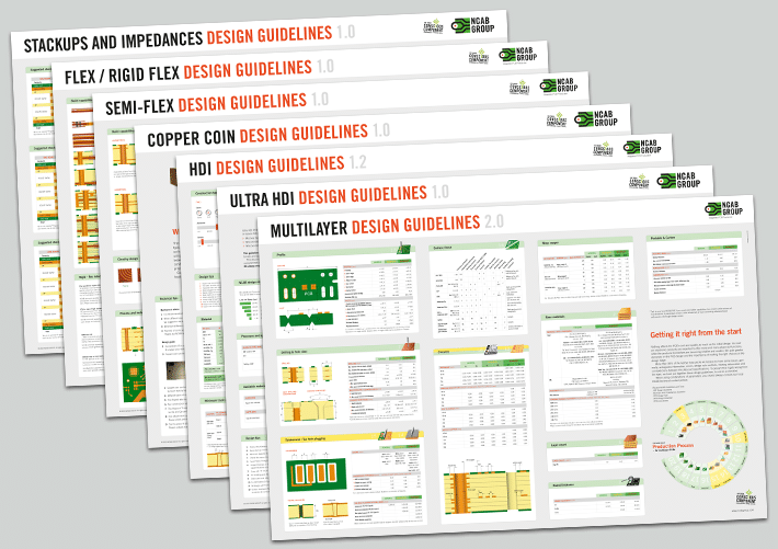
PCB design guidelines
Get it right from the start with our PCB design guidelines. To prevent getting it wrong from the start, we have put together our design guidelines, to use as a checklist.
