Recently I’ve been getting a lot of questions when we’re producing flex PCBs for customers. The questions revolve around materials and more specifically, when we have a plated through hole (PTH), why we need to implement PCB button plating on these designs. So, what is it and why is it needed?

First let’s discuss the basics when it comes to a typical rigid PCB. During the production process with a rigid PCB, we would image and etch our inner layer cores, laminate them together, drill and plate with Electro Deposited copper (ED copper), and then move on to pattern plating. So you have copper foil with essentially three additional copper deposits on top of it.
With flex PCBs it’s different. We don’t want to stack a ton of copper over our pattern because it reduces flexibility, which is the objective when creating a flex PCB. Also, the type of copper material is different. Flex PCBs uses a base copper of Roll Anneal (RA copper). This has a horizontal, linear grained structure and when it’s bent, it doesn’t have the tendency to fracture. ED copper has a more granular grain structure. If we plated it like we did a traditional multilayer PCB, we’d be stacking ED copper on top of that and the result is a dissimilar copper grain structure. Where RA copper is intended to bend and where ED copper is not, you could in theory have reduced flexibility or potentially a defect with the copper partially fracturing or failing to bond to itself.
When is PCB button plating needed?
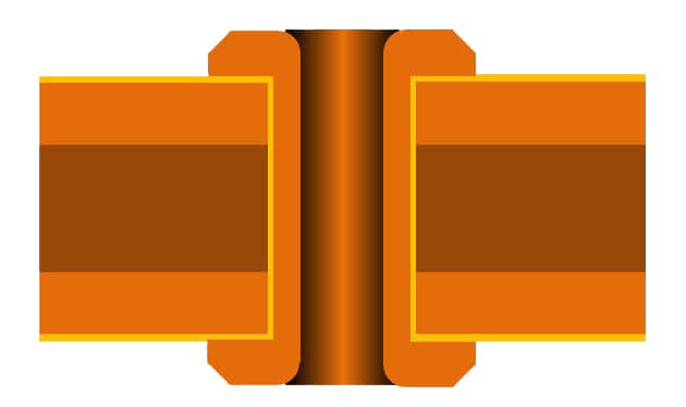
That brings us to the need for button plating. Whether it’s to support a dynamic bending application by allowing for a single deposit of RA copper or facilitating higher speed impedance control by supporting a homogenous base copper. In the process of button plating we only plate the areas of the PTH (plated through hole) and supporting pads. The term button plating refers to the visual aspect of the final product. If you were to look at the cross-section, you would see your flat surface and then you would have what looks like buttons as the PTH is slightly raised from the other copper features. The process is done by selectively masking the areas which do not receive the plating, allowing the plating chemistries to only access the areas of the PTH. We’re putting copper in the PTHs, we just sometimes do it differently between flex PCBs and rigid PCBs.

This process can also be utilized in some cases for other types of technology where a heavier deposit is required in the PTH but not across the entire surface of your outer layers. An example of this could be .002” minimum through hole plating with a design not intended to support heavy copper. I would be cautious with this technology as such a process can be demanding on the PCB manufacturer and in turn a significant cost driver.
Smaller line width and spacing possible
A potential added benefit to PCB button plating is the ability to have smaller line width and spacing. Since the increase in miniaturization, many times a flex PCB is built to be in a smaller space. Although this is not always the case. I’ve built flex boards that are almost two feet long. If you visualize the copper plating process on a multilayer PCB, we’re including the plating on all features, and all the circuitry is going to get that additional plating on it. So we’re plating in a 3-dimensional trapezoidal shape from the top as well as the sides. All the features that are close together get even closer as we plate them.
1 mil difference could mean all the difference.
On a flex PCB, because we use button plating, once you image and etch, the circuitry is done. The plating process does not further reduce any spacing. This allows us to achieve finer features. For reference, on a multilayer PCB, we’re limited at about 2.99 mils line, width and spacing. With a flex PCB we can get around 1.99 mils. Although this is just 1 mil difference, depending on the design, this could really mean all the difference. The design can be smaller which supports miniaturization and the ability to have smaller features closer together.
So there you have it. Rigid PCBs and flex PCBs often utilize different materials and employ a different production process. This is important to keep in mind during the design and procurement stages of producing a PCB. If you’re new to flex PCBs, more than likely you’ll want a different fabricator than a fabricator producing traditional multilayer PCBs. Another benefit to working with us at NCAB Group, as we produce a high mix of various technologies, we are always able to provide design support and source the right factory for the right design, getting it right from the start.

PCB design tools
For more advice about PCB design or applications of PCBs, we
have different PCB tools that can be downloaded for free.
