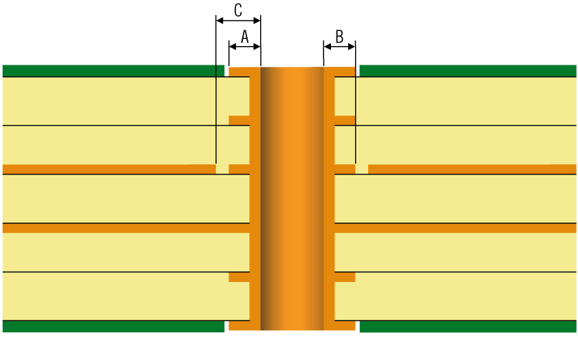
Why is there a demand for such a big distance from hole edge to copper for non-plated holes (NPTH)?
When you drill holes in the circuit board you want to drill all holes in the same set up to get the best position accuracy for the holes. The non-plated holes needs then to be blocked during the plating process (otherwise they will be plated as well). To be able to block the NPTH we need space between the hole edge and copper. The distance needed is related to the copper thickness. For standard copper thickness (18µm base copper), a good value is 0,3mm and definitely not less than 0,2mm.
What does same net spacing mean?
“Same net spacing” means that the copper to copper distance within the same electrical net is too close to be able to produce according to the Gerber files. Since it is within the same net, the DRC (design rule check) in the customer CAD software doesn´t alarm for this failure. It is important that the customer set the limits correct when starting a new design. Minimum copper to copper distance is normally set up correct, but they miss to set the same value when within the same net. It is not a very big issue, but it causes delay and unnecessary technical questions.
Should we remove or keep non-functional pads?
It’s clearlydefined in IPC-2222A point 9.1.4 that the fabricator shall not remove these,but many factories ask they allowance to remove these to achieve a better yieldin production. If they are not critical for the function, werecommend consider allowing their removal.

How much finished copper can be expected?
There is a misperception that copper weights offer certain exact thicknesses and that these do not reduce during the production of a PCB. For example 1 oz. = 35um or ½ oz. = 18um.
However IPC-6012 detailed the acceptable minimum thickness of both copper foils and foils after plating based upon allowable tolerances of copper foils and reductions of plating copper during subsequant processing.
Below shows some of the more standard copper weights and allowable finished thickness.
As such it is critical to understand what you need and specify correctly – if not then you may under-specify or you may over-specifiy which can lead to excess costs being built into the design. For more information, please consult our technicians.
| Inner layer foil thickness after processing | |
| Base copper weight | Minimum finished after processing |
| 1/2 oz. | 11.4 um |
| 1 oz. | 24.9um |
| 2 oz. | 55.7um |
| External conductor thickness after plating and processing | ||
| Base copper weight | Minimum finished after processing Class 2 | Minimum finished after processing Class 3 |
| 1/2 oz. | 33.4um | 38.4um |
| 1 oz. | 47.9um | 52.9um |
| 2 oz. | 78.7um | 83.7um |
When I need thicker tracks than standard, which track widths can I use?

In general, the thicker the copper base, the wider the track should be. One rule of thumb is that with a 18 µm copper base the track should not be narrower than 0.1 mm (4 mil) and with a 105 µm copper base the track should not be narrower than 0.25 mm (10 mil).
What is the minimum pad size hole on the outer/inner layer?
This varies from manufacturer to manufacturer, but in general you can say that the majority of manufacturers can produce them as follows:
A = 0.15 mm
B = 0.20 mm
C = 0.30 mm

