HDI
What is a microvia?

According to the new definition within IPC-T-50M a microvia is a blind structure with a maximum aspect ratio of 1:1, terminating on a target land with a total depth of no more than 0.25mm measured from the structure’s capture land foil to the target land.
The IPC-6012 also defines the structure of a Microvia.
- The Microvia is a blind structure with a maximum aspect ratio of 1:1 between hole diameter and depth, with a total depth of no more than 0.25 mm, when measured from the surface to the target pad or plane.
- Typically NCAB considers the dielectric thickness between surface and reference pad to be 60 – 80um.
- The diameter dimensions of the microvia have a range of 80-100 microns. The typical RATIO is between 0.6: 1 to 1: 1, ideal 0.8: 1
Would you like to learn more about microvias?
What is meant by a blind via hole?
A blind via hole is a hole that runs from an outer layer to the inner layer, but not through the entire PCB. These holes can be drilled mechanically or using laser technology. The image shows a laser drilled blind via.

Would you like to learn more about microvias?
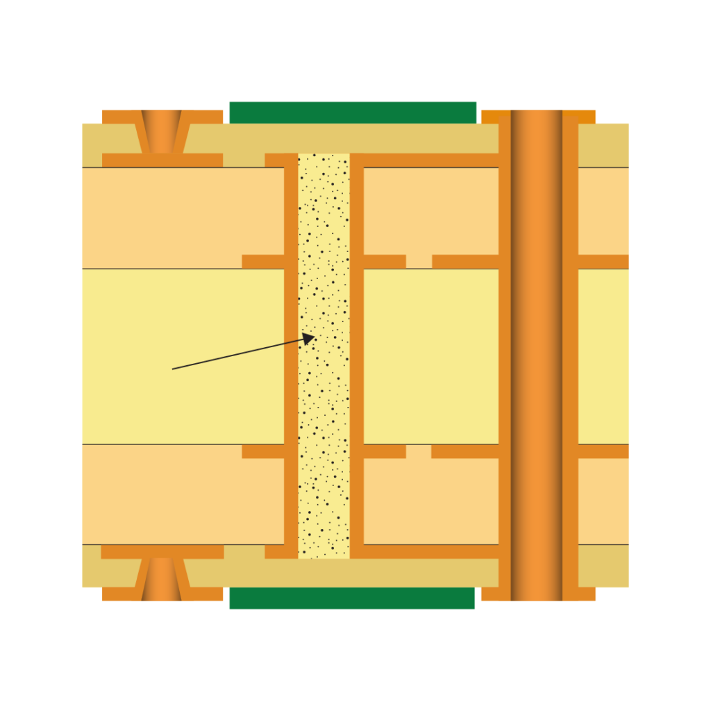
What is meant by a buried via hole?
This is a hole that runs between one or more inner layers. They are normally mechanically drilled.
Would you like to learn more about microvias?
What is a HDI PCB?
IPC-2226 defines HDI as a printed circuit board with a higher wiring density per unit area than conventional printed circuit boards (PCB). They have finer lines and spaces ≤ 100 µm / 0.10mm, smaller vias (<150 µm) and capture pads <400 µm / 0.40mm, and higher connection pad density (>20 pads/cm2) than employed in conventional PCB technology.
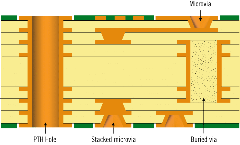
Are there different types of HDI features?
The graphic below shows the main structures – type I, type II and type III as defined in IPC-2226.
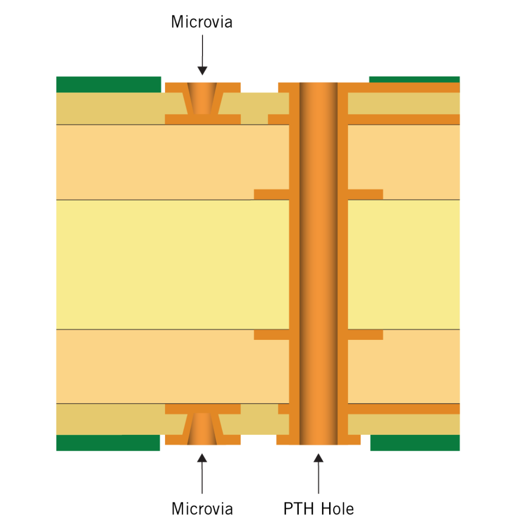
Type I. Defines a single microvia layer on either one or both sides of core. Uses both plated microvia and PTH for interconnection, employing blind, but not buried vias.
Type II. Defines a single microvia layer on either one or both sides of core. Uses both plated microvia and PTH for interconnection. Employs blind and buried vias.
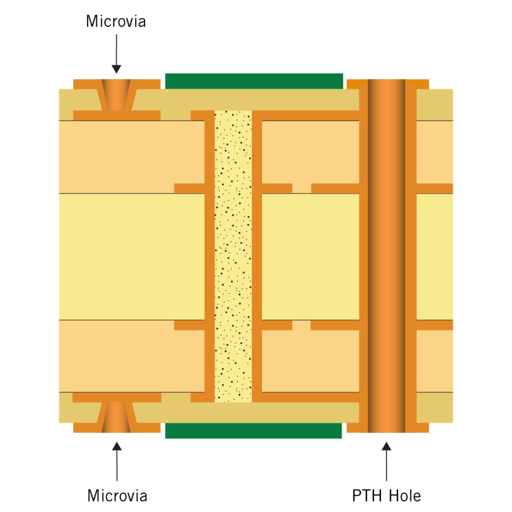
Type III. Defines at least two layers of microvia on either one or both sides of core. Uses both plated microvia and PTH for interconnection. Employs blind and buried vias.
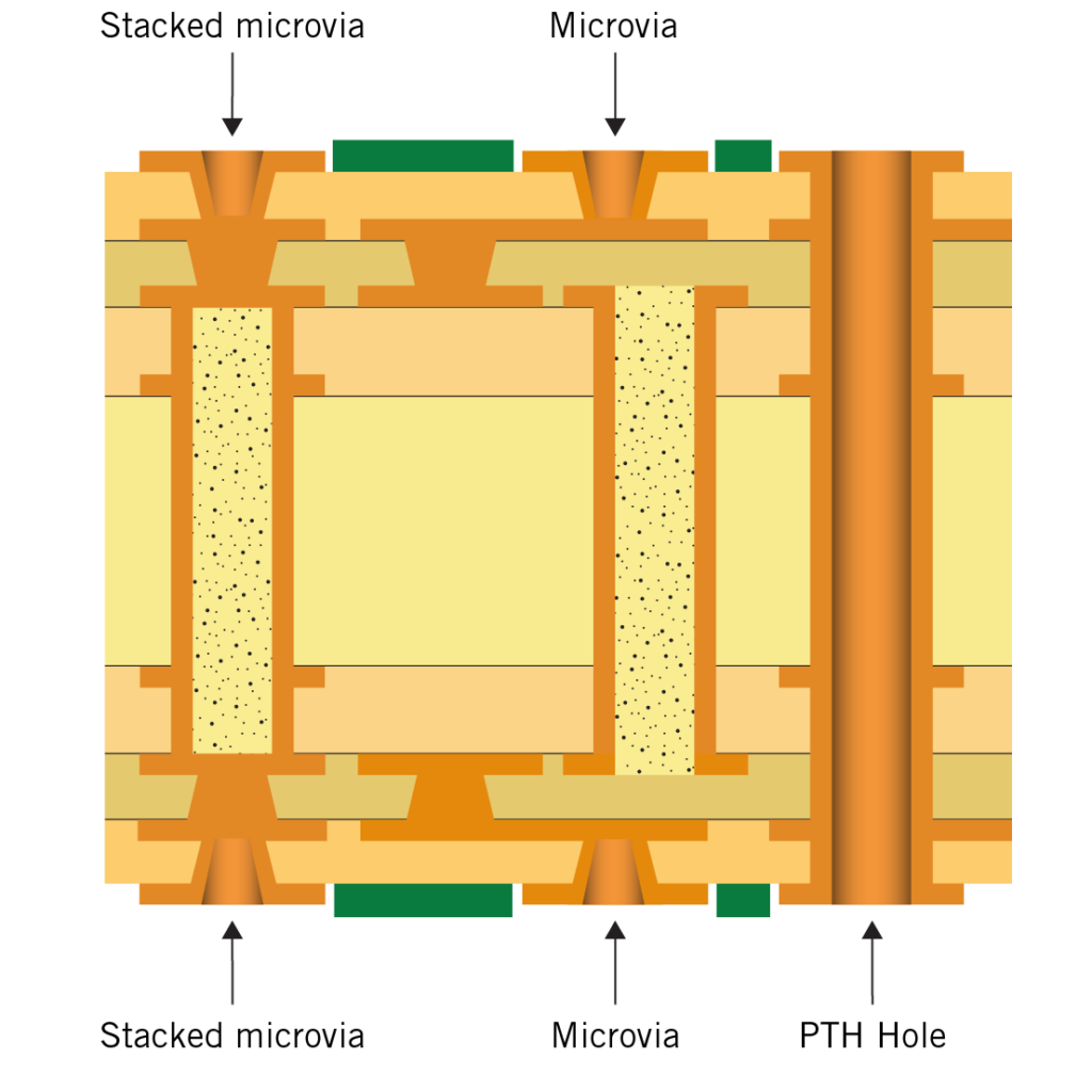
Construction terminology to define the degree of HDI construction:
- 1+n+1 = single layer of microvia (as per the type I and type II examples above)
- 2+n+2 = 2 layers of microvia (as per the type III example above)
- 3+n+3 = 3 layers of microvia
Learn more about HDI PCBs
What is Ultra HDI PCB?
To be defined as an Ultra HDI PCB, the circuit board must have:
- Conductor width and isolation distance below 50 µm
- Dielectric thickness below 50 µm
- Microvia diameter below 75 µm
- Product characteristics that exceed the existing IPC 2226 level C standard
Learn more about Ultra HDI in this video.
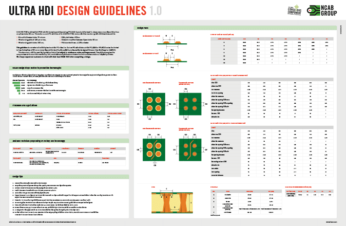
Design guidelines for ultra HDI
Download our PCB design guidelines for Ultra HDI to get your design right from start.
More information about Ultra HDI PCBs
FLEX/RIGID-FLEX
What are the available structures for flex and rigid flex PCBs?
There are numerous, different structures available. The more common ones are defined below:
Single sided flex (IPC-60103 type 1) Coverlay (polyimide + adhesive) bonded onto an adhesiveless single sided FPC core. With or without stiffeners.

Double sided flex (IPC-6013 type 2) Coverlay bonded onto both sided of an adhesiveless double-sided FPC core (two conductive layers) with plated through holes. With or without stiffeners.

Multilayer flex (IPC-6013 type 3) Coverlay bonded on both sides of an adhesiveless construction containing three or more conductive layers with plated through holes. With or without stiffener. Capability is 4L.

Traditional rigid flex construction (IPC-6013 type 4) Multilayer rigid and flexible circuit combination containing three or more layers with plated through holes. Capability is 22L with 10L flex layers.

Asymmetrical rigid flex construction, where the FPC is situated on the outer layer of the rigid construction. Containing three or more layers with plated through holes.

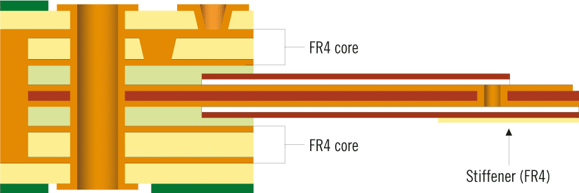
Multilayer rigid flex construction with buried / blind via (microvia) as part of the rigid construction. 2 layers of microvia are achievable. Construction may also include two rigid structures as part of a homogeneous build. Capability is 2+n+2 HDI structure
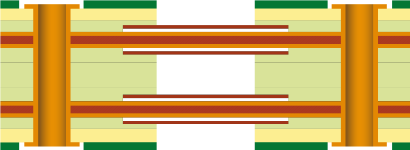
Book-binder and air-gap build – a complex build. With spaces between layers of flex to allow for improved flexing of the FPC. Flex layers may be of different lengths on the book-binder constructions to minimize compression of inner flex layers within bend radius.
How do you calculate correct length of flex part of a rigid flex structure to allow for minimum bend radius?
Detailed recommendations can be found in IPC-2223, sections 5.2.3.3 for both static and dynamic bends and should be used for final design verification. However, some basic guidelines based upon the thickness of the flex material can be seen below:

| FLEX TYPE | MINIMUM BEND RADIUS |
|---|---|
| Single sided flex | 3 – 6 x circuit thickness |
| Double sided flex | 7 – 10 x circuit thickness |
| Multilayer flex | 10 – 15 x circuit thickness |
| Dynamic application | 20 – 40 x circuit thickness |
What is the difference between semi-flex and rigid flex?
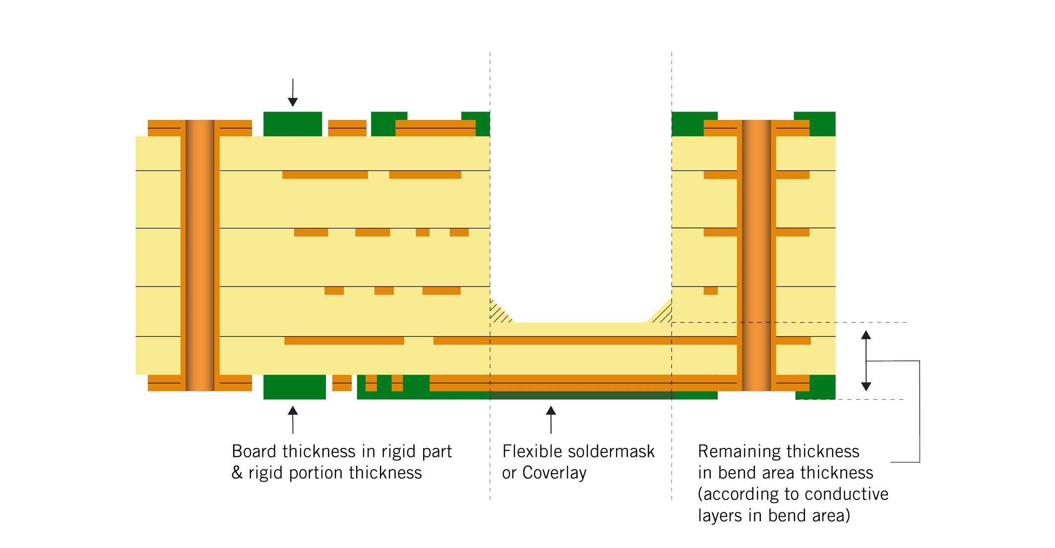
Semi flex is effectively a ‘standard’ multilayer PCB, built using specific types of FR4 that has been depth to a specific tolerance so that the resulting thinner area provides a flexible / bending section of the traditionally rigid FR4.
Semi flex is suitable for static applications (flex to install), or with very limited number of bends.
What is the difference between adhesive and adhesiveless flex systems?
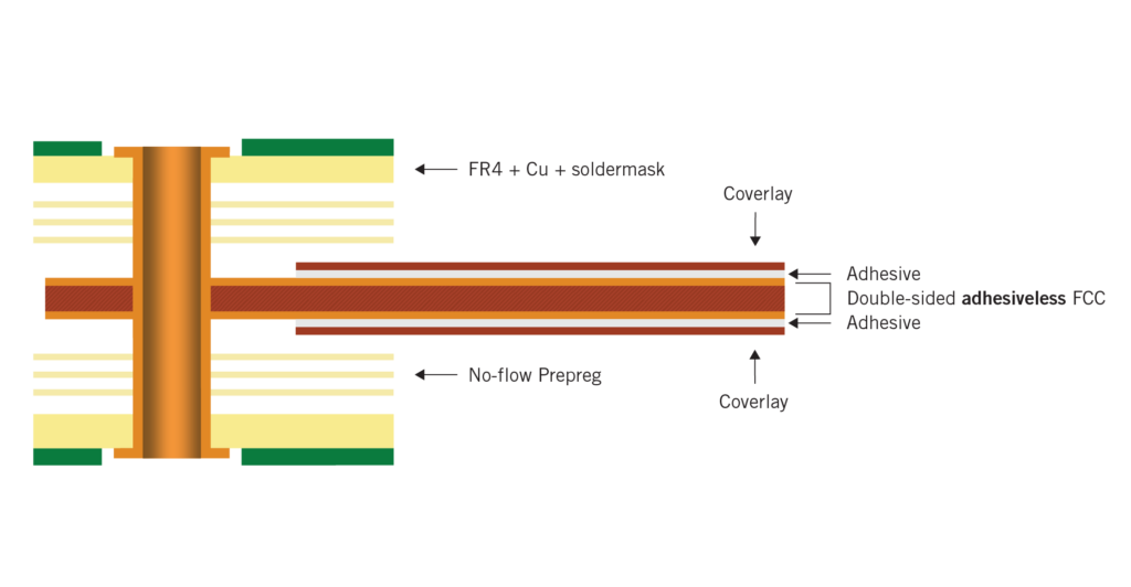
Builds that use adhesive systems rely on adhesive to bond the copper to the flex core. As such this adhesive layer along with full coverlay, penetrates into the rigid construction and directly into the hole. The greater expansion coefficient of the adhesive increases the risk of through hole problems, such as cracks and via hole failures as a result of the expansion, while having this material within the hole itself can lead to hole wall copper formation issues resulting from poor desmear of adhesive.

The solution to improving via / through hole reliability was to move towards an adhesiveless copper clad system (copper bonded directly to the polyimide) and limit the overlap of the coverlay into the rigid part of the board. This ensures a much more reliable through hole structure without adhesive penetrating into the hole. This is by far the most common approach to rigid flex.
DESIGN RULES
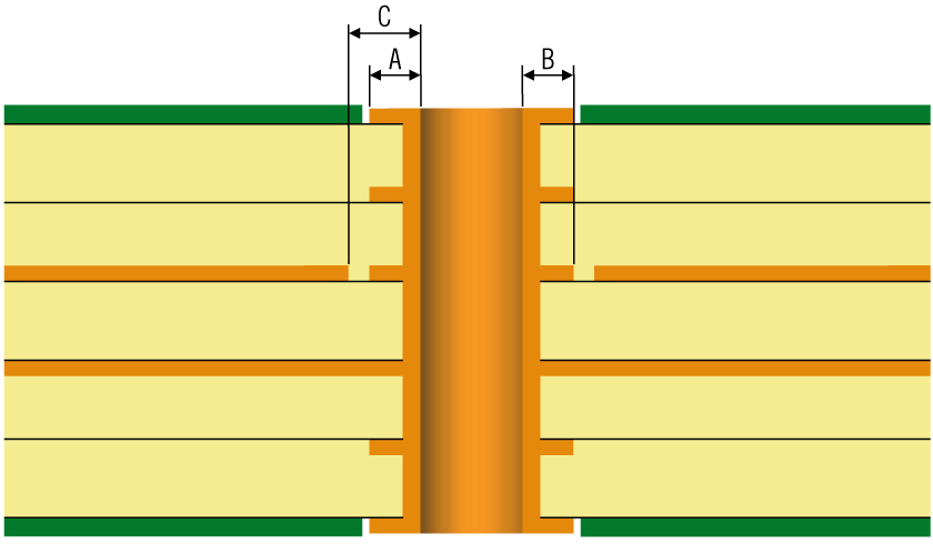
What is the minimum pad size hole on the outer/inner layer?
This varies from manufacturer to manufacturer, but in general you can say that the majority of manufacturers can produce them as follows:
A = 0.15 mm
B = 0.20 mm
C = 0.30 mm
When I need thicker tracks than standard, which track widths can I use?

In general, the thicker the copper base, the wider the track should be. One rule of thumb is that with a 18 µm copper base the track should not be narrower than 0.1 mm (4 mil) and with a 105 µm copper base the track should not be narrower than 0.25 mm (10 mil).
How much finished copper can be expected?
There is a misperception that copper weights offer certain exact thicknesses and that these do not reduce during the production of a PCB. For example 1 oz. = 35um or ½ oz. = 18um.
However IPC-6012 detailed the acceptable minimum thickness of both copper foils and foils after plating based upon allowable tolerances of copper foils and reductions of plating copper during subsequant processing.
Below shows some of the more standard copper weights and allowable finished thickness.
As such it is critical to understand what you need and specify correctly – if not then you may under-specify or you may over-specifiy which can lead to excess costs being built into the design. For more information, please consult our technicians.
| Inner layer foil thickness after processing | |
| Base copper weight | Minimum finished after processing |
| 1/2 oz. | 11.4 um |
| 1 oz. | 24.9um |
| 2 oz. | 55.7um |
| External conductor thickness after plating and processing | ||
| Base copper weight | Minimum finished after processing Class 2 | Minimum finished after processing Class 3 |
| 1/2 oz. | 33.4um | 38.4um |
| 1 oz. | 47.9um | 52.9um |
| 2 oz. | 78.7um | 83.7um |
Should we remove or keep non-functional pads?
It’s clearlydefined in IPC-2222A point 9.1.4 that the fabricator shall not remove these,but many factories ask they allowance to remove these to achieve a better yieldin production. If they are not critical for the function, werecommend consider allowing their removal.

What does same net spacing mean?
“Same net spacing” means that the copper to copper distance within the same electrical net is too close to be able to produce according to the Gerber files. Since it is within the same net, the DRC (design rule check) in the customer CAD software doesn´t alarm for this failure. It is important that the customer set the limits correct when starting a new design. Minimum copper to copper distance is normally set up correct, but they miss to set the same value when within the same net. It is not a very big issue, but it causes delay and unnecessary technical questions.
Why is there a demand for such a big distance from hole edge to copper for non-plated holes (NPTH)?
When you drill holes in the circuit board you want to drill all holes in the same set up to get the best position accuracy for the holes. The non-plated holes needs then to be blocked during the plating process (otherwise they will be plated as well). To be able to block the NPTH we need space between the hole edge and copper. The distance needed is related to the copper thickness. For standard copper thickness (18µm base copper), a good value is 0,3mm and definitely not less than 0,2mm.
TERMINOLOGY
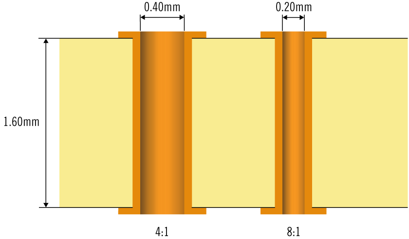
What is the “aspect ratio”?
The relationship between the diameter of the hole and its length. When a manufacturer states that their production has an “aspect ratio” of 8:1 it means, for example, that the hole’s diameter is 0.20 mm in a 1.60 mm thick PCB.
For HDI structures, the aspect ratio for microvia is limited to 1:1, but 0.7-0.8:1 is preferable to easy the plating.
What is copper wrap?
Copper wrap is a continuous deposit of plated copper that is deposited within the barrel of the hole and extends onto the surface of the PCB (or the surface of the innerlayer core if part of a HDI structure) by a minimum of 25 um.
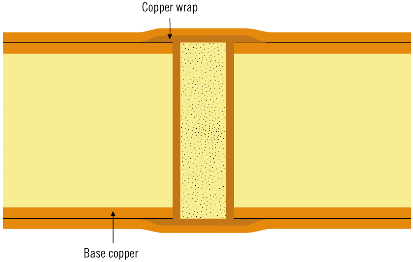
For class 2 demands the thickness of the surface deposit of the copper wrap is minimum 5um, but for class 3 demands this will vary dependant upon where this feature is situated within the build. Please consult our technicians for further information on class 3 demands.
What is a copper coin PCB?
A copper coin is a multilayer PCB but with the addition of a solid piece of copper, called a coin, embedded into the PCB’s stack-up. This allows a direct thermal connection from one side to the other or from a specific layer to an outer layer. Learn more in the video.
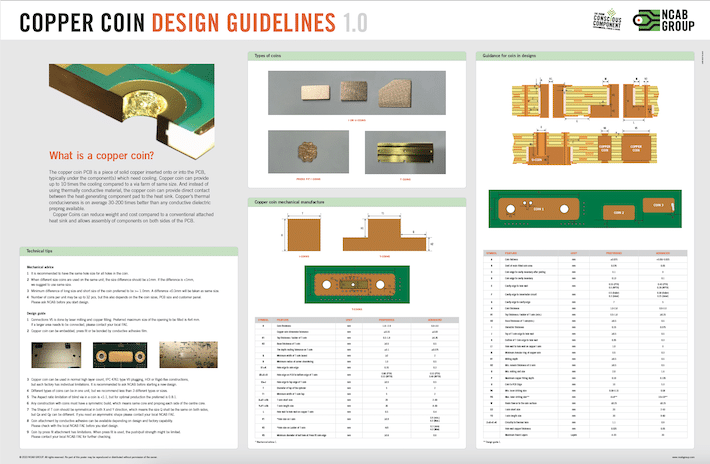
Design guidelines for copper coin
Nothing affects the PCB’s total cost and reliability as much as the initial design. That is why we have put together our PCB design tools for engineers, designers and anyone else involved in the PCB design or production process.
Design guidelines for Multilayer PCB, HDI PCB, Ultra HDI PCB, Flex / Rigid-Flex PCBs, Semi-Flex PCB, Copper coin and Stackups and Impedances are available for download.
Learn more about copper coin
Copper coin PCBs – efficiency and reliability in thermal PCB management
The overall goal of thermal management at the bare board and assembly level is to move the heat away from the heat-generating components to an external heat sink for dissipation. Better heat transfer will usually translate to lower mean time between failures (MTBF) and at times will be a deciding factor at meeting product design specifications.
In this blog post we want to dive deeper into the growing technology of Copper Coin PCBs. Heat transfer occurs at a higher rate when materials of high thermal conductivity are used. Copper is extremely conductive offering upwards of 400 W/mK, as is for example other materials like diamonds, which can be up to five times more thermal conductive than copper. But, who wants to use diamonds in their PCBs? Copper is one of the best ways to manage heat while keeping electrical and or thermal conductivity.
What is controlled impedance?
Consider the PCB signal as it travels along a track controlling impedance means that we control the performance or speed of that signal at a point along a track. Related to resistance, capacitance and conductance of the track in question. The impedance is also measured in Ohms, it is different than resistance which is a DC characteristic. Impedance is an AC characteristic, meaning that it is related to frequency.
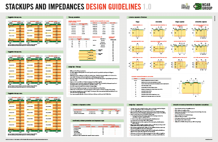
Design guidelines for stackups and impedances
Download our PCB design guidelines for Stackups and Impedances to get your design right from start.
Is there more than one type of controlled impedance?
Yes, there isand these are explained below:
Differential impedance – Impedance of a pair of conductors with equal and opposite polarity signals – same amplitudein anti-phase with each other.
Odd mode impedance – Impedance of one side of a pair of conductors which both have equal and opposite polarity signals – same amplitude and anti-phase.
Even mode impedance – Impedance of one side of a pair of conductors which have equal signals – same amplitude and same polarity.
Common mode impedance – Impedance of a pair of conductors which have equal signs – same amplitude and same polarity.
Learn more about impedance

Design guidelines for stackups and impedances
Download our PCB design guidelines for Stackups and Impedances to get your design right from start.
What is meant by a thermal pad?
For SMD components, especially the smaller ones, use thermal relief pads to simulate the same thermal mass on both terminations to avoid tombstoning, twisted components or even in worst case broken components.
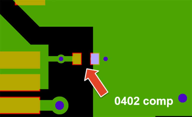
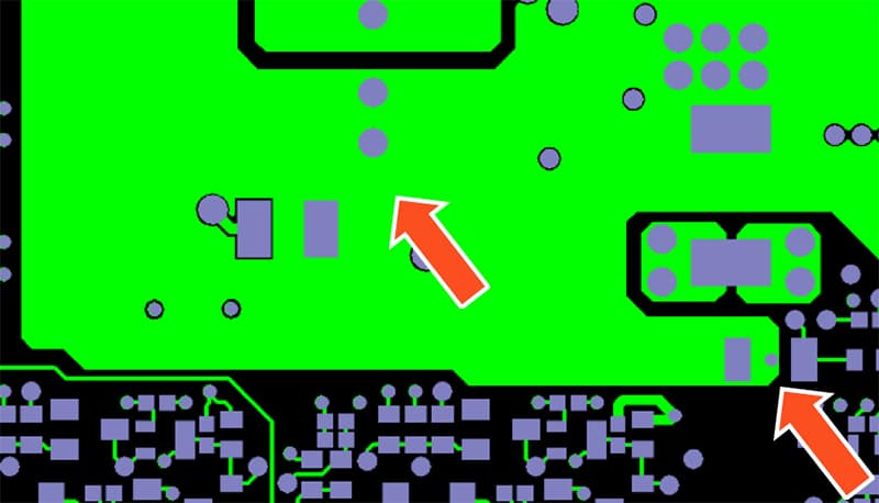
For hole mounted (HMD) components we use thermal relief pads on inner layer planes to help wetting in the hole barrel. Formulas for thermal relief pads can be found in IPC-2220 series.
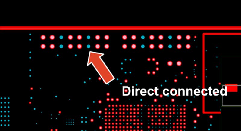
Should approval for addition of teardrops be added in the procurement documentation?
According to new IPC-6012D section 3.4.2 it is allowed to add teardrops to the tracking when boards shall comply to classes 1 & 2.

If you do not want tear-drops, highlight that in the procurement documentation. But add enough annular ring.
What is back-drilling technology?
For high frequency applications we need to prevent signal loss and therefore when one layer is connected to another and the signal travels from one layer to another it must pass through a via hole that connects the layers. If the signal is to pass layer one to layer two in a 20 layer board, for example, then part of the via structure is considered as ‘excess’ and for this application it is best to remove the excess copper from this hole as it acts as an antenna and impacts the signal.
We use back-drilling (controlled depth in z-axis) to drill out the ‘excess’ copper in the hole in order to get better signal stability. Ideally the shorter the stub (‘excess’ copper) then the better the result. Back-drill size should be typically 0.2mm larger than corresponding via.
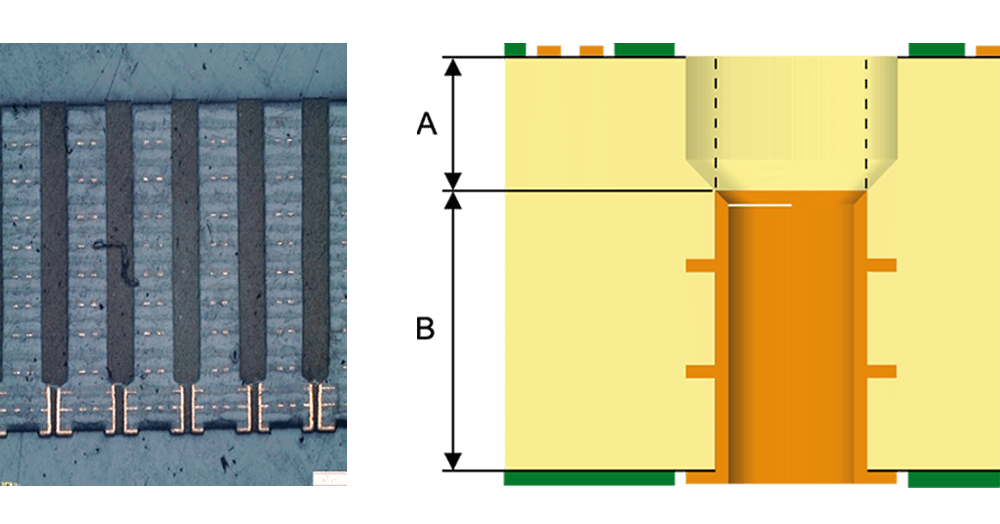
| BACK DRILLING / COUNTER BORE (mm) | |||
|---|---|---|---|
| A: Depth tolerance | +/-0.20 | +/-0.15 | +/-0.10 |
| B: Min. remain thickness and tolerance | 0.5+/-0.25 | 0.35+/-0.1 | 0.3+/-0.1 |
What does “UL marking” mean?
Security is keyin the electronics industry. It is vital that users can rely on the finished product when considering factors such as fireand electrical safety, which means that both the PCB and the materials theycontain must measure up to the highest standards. To ensure that the boards doconform, it has become common practice to UL certify the constituent materialsor the PCB itself.
To start with, what is UL? The letters UL stand for Underwriters Laboratories.
Why is UL recognition important? UL is a major authority and enjoys a good reputation in the PCB industry. The company is irreplaceable for testing fire and electrical safety. Customers from around the world – including well-known Chinese companies – demand factories that can achieve UL recognition. Having UL recognition is therefore very important for PCB factories to produce secure boards and be able to access the international market.
What is thermal resistance?
In this video you can learn about thermal resistance and thermal conductivity.
VIA HOLE
What type of via hole plugging is recommended?
The preferred type of plugging for standard product (not including capped via hole) is IPC 4761 type VI filled and covered, with target being complete fill. The image below shows type VI with liquid soldermask coverage.

Single sided plugging is not recommended (including type II tented and covered) due to concerns over entrapment of chemistry or likelihood of solderballs being present with HASL finishes (LF and SnPb).
Learn more about microvias
What is a capped via hole?
A capped via is when plating is added over the via hole so that the surface is fully metalized with a minimum copper / cap plating thickness of 5um for class 2 demands, or 12um for class 3 demands.
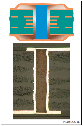
This is reliant upon the via filling material being epoxy resin as opposed to soldermask, as the epoxy will minimize the risk of air bubbles or expansion of the fill during soldering operations.This can be categorized within IPC-4761 as type VII – filled and capped via holes. It is typically used for designs with via in pad or in BGA applications where high density features are required.
More about microvias
MATERIAL
Do I have to use an FR4 material with a high Tg for lead-free soldering?
No, it´s not necessary to use a FR4-material. There are many factors to be taken into account, e.g. how many layers, the thickness of the PCB and also a good understanding of the assembly process (number of soldering cycles, time above 260 degrees, etc.). Some research has shown that a material with a “standard” Tg value has even performed better than some materials with a higher value. Note that even with “leaded” soldering the Tg (Tg = glass transition temperature) value is exceeded.
What is of most importance is how the material behaves at temperatures above the Tg value (post Tg) so knowing the temperature profiles the board will be subjected to will help you look evaluate the necessary performance characteristics.
What are the material characteristics to look for when selecting material?
The main ones that we would consider first include:
CTE
A measure of how much the material expands when heated. Critical in Z-axis – typically above Tg and the expansion is greater. If CTE insufficient for then failures can occur during assembly as the material expands rapidly above Tg.
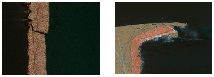
Materials can have same Tg yet different CTE’s – lower CTE is better. Equally some materials can have higher Tg values, yet also have a higher (worse) CTE post Tg.
Tg / GLASS TRANSITION TEMPERATURE
The Tg value is the temperature at which the material changes from a reasonably stiff glass-like material to a more elastic and bendable plastic-like material. Important as above Tg, the materials properties will change.
Td / DECOMPOSITION TEMPERATURE
This is a measure of the degredation of the material. The analysis-method measures when 5 % of the material is lost by weight – the point as which reliability is compromised and delamination may occur.
Higher reliability PCB will require Td ≥ 340℃
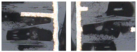
T260 / T288 / TIME TO DELAMINATION
This is the method to determine the time when the thickness of the PCB is irreversibly changed at a predefined temperature (260 or 288 in this case) – i.e. when the material expands to such a degree that it delaminates.
Do I have to use an FR4 material with the highest Td (Td = decomposition temperature) for lead-free soldering?
A greater Td value is preferable, especially if the board is technically complex and exposed to a number of remelting solderings, but this can lead to higher costs. Knowing your assembly process can help make the right choices.
What is the difference between “Dicy” and “nonDicy” as a hardening system in the FR4 epoxy?
Dicy (Dicyandiamine) is by far the most common hardening system for this epoxy; it normally gives a Td value of about 300–310°C while a “nonDicy”, i.e. a Phenolic Cured Epoxy has a Td value of about 330–350°C and can therefore better resist the higher temperature.
What does “CAF” mean?
CAF (Conductive Anodic Filament) means that there will be an electrochemical reaction between the copper anode and cathode, which may result in an internal short circuit in the material.
Which PCB surface is best for lead-free soldering?
There is no “best PCB surface;” all surfaces have their pros and cons. Which one you should choose depends on many factors. Please consult our technicians or review the information on surface finishes within this section of the website.
What are the rules regarding flame retardants, was there a national ban against TBBP-A which dominates in electronics?
No, the investigation found that it is, for practical reasons, not possible to ban.
What is the difference between flame retardant added in reactive or additive form?
Reactive flame retardant is chemically bound to the epoxy and will not dissolve and migrate out of the product as part of the waste deposit.
How many reflow cycles can FR4 materials withstand?
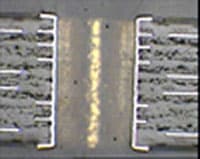
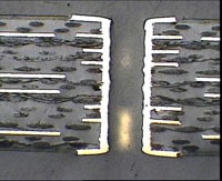
It is hard to give a precise answer, but we have made tests with material with up to 22 reflows, four of these with a peak temperature of 270C°. The stress after 22 reflows is considerable and material can degrade, but all connections remained functional. Our recommendation is to choose a higher grade material where there are more than 6 layers and thicker than 1.6 mm.
RoHS
Do the RoHS or WEEE directives require the PCB to be marked?
No, but for practical reasons PCBs that have lead-free HASL should be clearly marked stating their RoHS compatibility due to the risk of confusion with leaded HASL.
Are RoHS compatible PCBs also halogen-free?
No, not necessarily. The RoHS directive prohibits two bromided flame retardants, PBB (polybromided biphenyls) and PBDE (polybromided diphenyl ethers). What is normally used in PCBs is a bromided flame retardant called TBBP-A (Tetrabromobisphenol A).
