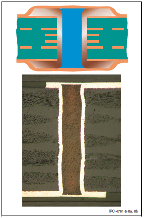
A capped via is when plating is added over the via hole so that the surface is fully metalized with a minimum copper / cap plating thickness of 5um for class 2 demands, or 12um for class 3 demands.

This is reliant upon the via filling material being epoxy resin as opposed to soldermask, as the epoxy will minimize the risk of air bubbles or expansion of the fill during soldering operations.This can be categorized within IPC-4761 as type VII – filled and capped via holes. It is typically used for designs with via in pad or in BGA applications where high density features are required.
