Electronic products are becoming more and more complex. The miniaturization of electronic components pushes the evolution of printed circuit boards towards complexity that was unthinkable only a few years ago.
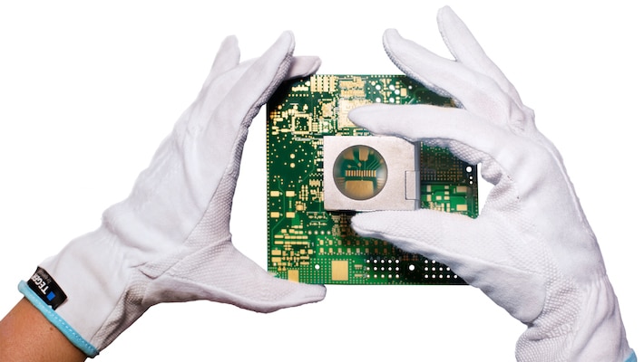
The need arises when one no longer thinks of an object that has a single and simple function, but of objects that are evolving in terms of performance and aesthetic appearance, and they have the ability to perform multiple functions and operations. The most classic example is the mobile phone. It transformed from a single function of making and receiving calls, to a system which connects everything around us.
Therefore, we are designing even smaller electronic boards, with more functions and performances all while being thinner and lighter. This requires a very rigorous design and production process to be able to obtain excellent performance. To develop what we have just described we need solutions for a greater density of connections and more layers in the printed circuit board.
The increasingly narrow design means less space available for routing, which results in thinner tracks and gaps with through holes of increasingly smaller diameter.
A couple notes on HDI designs:
- Blind holes are laser holes on the external sides
- Buried holes are laser holes to connect intermediate layers
- We also need thinner pre-preg and CCL laminates than conventional multilayer products
When the project is being taken to extremes, it is clear that the entire design process must follow some necessary guidelines, from the designer to the PCB supplier.
The internationally recognized IPC helps us a lot in defining these guidelines by referencing standards:
- IPC-2226 concerns the design section
- IPC-6012 concerns the acceptability section of rigid boards
- IPC-4104 covers the various conductive and dielectric materials that can be used for the fabrication of HDI
- IPC-4101 concerns the typical characteristics of the basic raw materials.
Definition of HDI circuit boards
In the IPC-6012 it is considered an HDI PCB when the electrical connections on average reach a number of 20 connections per cm2, on both sides of the core and generally to reach these conditions, microvia tracks and gaps should not exceed 100 um. If we think that the parameters described are developed on all layers of the circuit, we understand that it poses great technological challenges for PCB suppliers.
The IPC-6012 also defines the structure of a Microvia.

- The Microvia is a blind structure with a maximum aspect ratio of 1:1 between hole diameter and depth, with a total depth of no more than 0.25 mm, when measured from the surface to the target pad or plane.
- Typically NCAB considers the dielectric thickness between surface and reference pad to be 60 – 80um.
- The diameter dimensions of the microvia have a range of 80-100 microns. The typical ratio is between 0.6: 1 to 1: 1, ideal 0.8:1
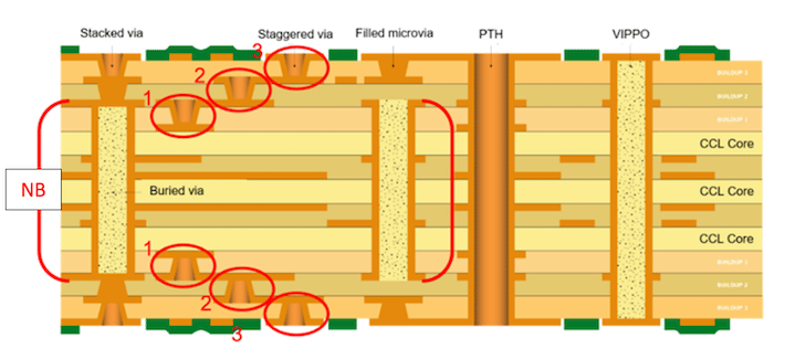
The IPC-2226 Defines the structures of HDI by type, there are three types and we can observe in the images highlighted:
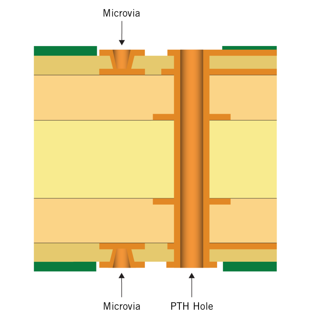
- TYPE 1 STRUCTURES are those that contain a single layer of microvia on one or both sides of the core. It uses both microvias and through holes for interconnection. It is important to keep the ratio 0.8: 1 for the microvia, this structure uses ONLY blind holes NO passage to buried holes.
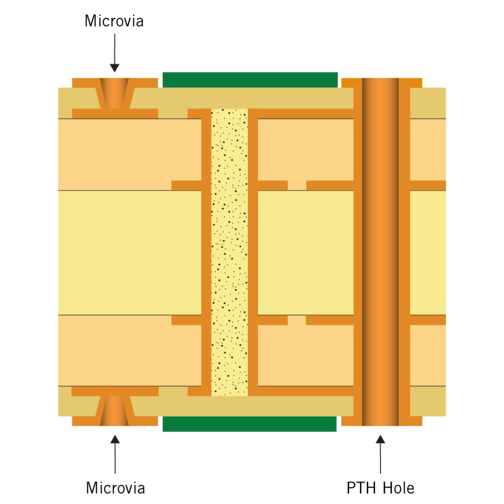
- TYPE 2 STRUCTURES are similar to type 1 in that they contain only a single layer of microvia on one or both sides of the core. It uses both microvia and through holes for interconnection, but unlike type 1 these structures also use buried holes.
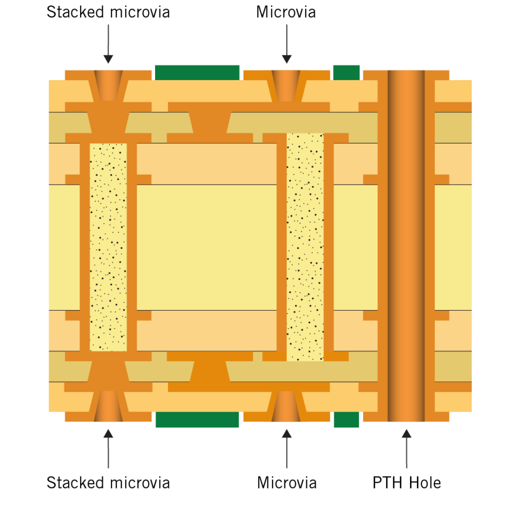
- TYPE 3 STRUCTURES are the most complex and demanding for factories, they contain AT LEAST two layers of microvia on one or both sides of the core. As for type 2, it also uses through holes in addition to blind and buried vias.
Why an HDI circuit board?
We already know what led us to this, it is the technology that is evolving, taking everything to the extreme in terms of compaction and miniaturization. But what are the advantages?
It is possible to obtain more complex designs in terms of space and interconnections and clearly use latest generation components – including BGA pitch 0.4 mm and smaller. These components need multiple connections in a very small space.
Returning to describe the types of microvia essential for an HDI construction, we can find examples in a Type III structure (Fig. 1), they are closely linked to parameters well-defined by the design rules.
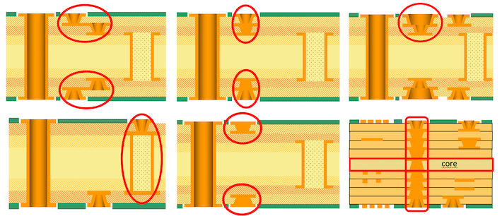
Microvias Staggered
These are staggered non-overlapping microvias. In this case the buried microvias do not need to be filled with the copper vias filling process
Microvias Stacked
These are overlapping microvias. In this case the buried microvia needs to be filled with copper, through the process of copper vias filling, a process widely used for this technology.
Microvias Stepped
These are overlapping microvias. This rather unusual construction and has the characteristic of having two different overlapping diameters of blind holes. For this structure it is not necessary to fill the first level of the blind holes with copper.
Microvias on Pad
For this type with vias on pad, the buried hole must always be filled with low CTE epoxy resins, then capped with copper. In this case we are talking about process according to IPC 4761 type VII.
Microvias filled on Pad
For this type the vias on pads are filled with the copper vias filling process. This allows the latest generation components with very fine pitch to be welded onto the same drilled pads.
Microvias ELIC
With this type, the microvias are overlapping , starting from a central core. The object is constructed sequentially using the laser drilling process and the copper vias filling process SBU (sequential build up).
Copper vias filling process
Why is this process important for an HDI PCB? Here we see the section results. The advantages are clear in terms of thermal dissipation and higher current load supported. Lately, the combination of implants and chemistry have contributed to a better flatness of the pads. This will allow, during the assembly of the components, a reliable welding of the latest generation components.
To have a good result the correct combination of process and design is important:
- Have a good laser hole, clean and free of protruding glass fibers.
- A very accurate control of desmearing and plating processes
- The diameter of the laser hole between 80-100µm.
- The dielectric thickness between 60-80 µm
- That in addition to allowing the right diameter of the hole, as we see in the photo, it will also give the possibility of having a dimple (depression) of a few µm on the drilled pad
A brief outline of the steps with the copper vias filling process:
- The chemistry contains a particular content between brighteners and leveling agents that allow you to fill the cavities of the blind hole.
- The brighteners act on the bottom accelerating the copper deposit.
- The leveler prevents deposit on the surface and allows sufficient flatness for welding via on pads.

Selection of Raw Materials
It is important to select the correct raw materials taking into account the main characteristics:
- Tg – Glass Transition Temperature
- CTE – thermal coefficient of Z axis expansion
- Td – Decomposition temperature
We have all heard about the Tg of a material. The value of Tg is the temperature at which the material transforms from a rigid material such as glass to a more elastic and flexible material such as plastic (Glass Transition Temperature). This value is important because going with the temperature beyond the value of Tg, the properties of the materials change and deteriorate.
CTE – Coefficient of thermal expansion, measures the expansion of the base material, essentially on the Z axis when heated and usually when the temperature is higher than Tg, the expansion is greater. If the CTE value stated in the material data sheet is too high, assembly failures can occur as the material can expand faster beyond the temperature of Tg. Materials can have the same Tg value, but with different CTEs. In this case, for the same Tg, it is preferable to choose a lower CTE value.
Decomposition Temperature (Td) is a measure of the degradation of the material. The analytical method measures the temperature at which the material loses 5% of its mass, at which point reliability is compromised and delamination phenomena can occur. A more reliable printed circuit requires a value of Td ≥ 340 ℃
For more information about HDI technology, contact the NCAB Group experts and we will be happy to support your needs.
Do you want to know more about PCB design?
Design guidelines for HDI
Download our PCB design guidelines for HDI to get your design right from start.
PCB design – what you need to know
We have collected everything you need to know about printed circuit board design in one page.
