These designs often require special materials, demand high reliabilty and expect good repeatability. More importantly, the whole electronics industry is more dynamic than ever, forcing customers to pay much more attention to faster time-to-market (TTM) due to fierce global competition. Not surprising then, Design for Manufacturability (DFM) in PCB design plays a crucial role in the whole product development cycle and getting it right first time!
Our research highlights some major issues which affect TTM:
30% of PCB designs have design errors
50% of customers are not sure at the design stage of which PCB factory to use
70% of customers do not know the impact their design has on volume production
A demand for a one-stop PCB supplier to provide turnkey PCB layout and manufacturing is a reality, mainly due to the vast array of PCB requirements that necessitate up-front technical support, cost reduction initiatives, and the assurance that quality standards will always be maintained at the highest level. This presents some challenges, especially in finding one PCB supplier who can take full responsibility from PCB layout right to volume production.
NCAB PCB Design+ was brought about to offer such a comprehensive service. With a well established reputation for high quality and high reliability PCBs, NCAB Group China now offers advanced PCB layout services to address the complex nature of modern PCB products.
Some of the benefits with using NCAB PCB Design+
PCB Material selection:
Choosing a suitable PCB material is often a balance between cost, performance, and quality. Often, Gerber files and instruction documents only describe the material as FR4. Truth be told, there are hundreds of variants of FR4 material available, with vastly different levels of quality and consistency. Choosing the wrong material for your specific product application, or not specifying clearly the key parameters of FR4 material to be used for your application, could be disastrous to the functioning of your PCB in the field. In addition, PCB factories do not always stock high performance or special materials.
Communicating at an earlier stage with us can prevent long leadtime and minimum order value (MOV) problems. Due to the one-stop in-house design and manufacturing, early on at the PCB layout stage we are able to advise on material selection, PCB stackup, impedance requirements, drill technologies, and cost reduction alternatives. This approach prevents nasty surprises later, or even worse a complete PCB re-design.
PCB stackup:
Often a PCB manufacturer is not able to build a PCB stackup designed by the PCB layout engineer. The main reasons are availability of base materials, unavailable copper thicknesses, too strict overall thickness tolerances, and unbalanced layers.
Planning the good multilayer stack-up is the most important factor in determining the EMC performance of a product. A well designed layer stack-up not only minimizes the energy it radiates, but can also make the circuit relatively immune from external noise sources. Well-stacked PCB substrates can also reduce signal crosstalk and impedance mismatch issues. On the other hand an inferior stack-up can increase the EMI radiation, because reflections and ringing in the system due to impedance mismatch which can dramatically reduce the product performance and reliability.
NCAB PCB Design+ engineers have an in-depth knowledge of PCB materials, they have immediate insight into material availability at the factories, and they have access to world-leading tools to verify power and impedance requirements. In addition, a library of common stackups is available on demand, tailored to material availability, technology levels of the factories, and volume capacity of the factories.
Live DFM support:
“Design for Manufacturability” is the process of designing a PCB layout to prevent problems that could be encountered during the PCB manufacturing and assembly processes required to manufacture an electronic system. Designs submitted without DFM defects are less expensive to manufacture than ones with DFM defects. Worse still, having a design that cannot be manufactured or which will cost more than budget, can cripple a company due to design re-spins.
Having insight into standard and advanced capabilities of the factories allows NCAB PCB Design+ engineers to ensure that correct choices are made up-front. With a full CAM and PPE support team, they are able to prevent common issues such as drilling aspect ratios, copper thicknesses and other criteria not common knowledge to PCB layout engineers in companies.
Other benefits:
Since NCAB PCB Design+ engineers have direct access to the factory’s ERP systems, your sample PCB will be made in the same factory as your future production volumes. Hence your product verification and certification can be done with the assurance that the production volumes will perform consistently as the samples.

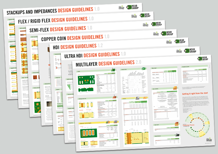
PCB design guidelines
Get it right from the start with our PCB design guidelines. To prevent getting it wrong from the start, we have put together our design guidelines, to use as a checklist.
