When it comes to printed circuit boards (PCBs) for the railway sector, one immediately thinks of the many standards imposed by this industry, such as EN 45545-2. However, meeting these requirements is not enough to guarantee PCB reliability. During manufacturing, it’s important to use the right parameters, equipment, and processes to ensure PCB reliability, especially for safety-related applications. At NCAB, we follow IPC requirements when manufacturing our printed circuit boards, some of which exceed IPC class 3 standards.
In this blog post, we will delve deeper into the four critical processes involved in PCB manufacturing for railway applications, highlighting how each process impacts the board’s performance and overall reliability.
1. Lamination influences many parameters
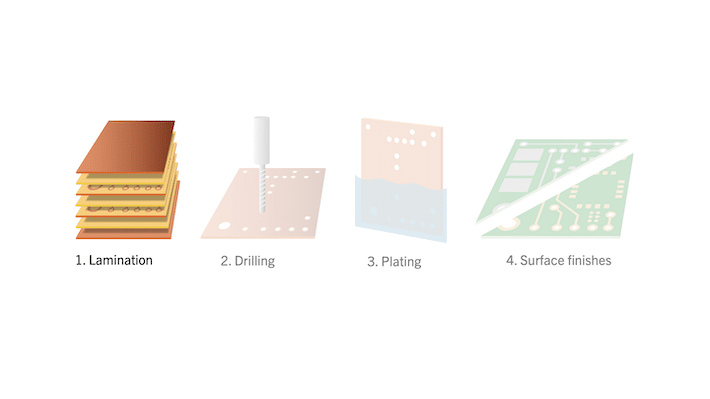
Lamination is an essential step in the manufacturing of PCBs. It consists of stacking different layers of material to form a multilayer printed circuit board. This process is important because, once completed, the PCB serves as the basis for all assembled components. Lamination can also affect PCB performance in the following ways:
a) Mechanical properties of the printed circuit board:
- PCB thickness, material and copper delamination resistance, bending strength, etc., are important mechanical properties.
- Resin flow is controlled by the parameters used during lamination. Different pressures, temperatures, and durations will result in different dielectric thicknesses, which will also affect impedance.
- The x/y expansion also affects the position accuracy of the pattern.
b) Internal stress relief
Internal stress relief is a key step during lamination. Internal stress can cause deformations such as bow and twist. Inter-layer alignment is crucial after lamination. Misalignment of the various layers can lead to dispersions in the position of the images, and therefore in the accommodation ranges of the components.
c) Thermal reliability
The glass transition point (Tg) is checked after lamination. This is the temperature at which the material becomes softer. Some materials with a low Tg present a risk of delamination. Upstream of the lamination process, control of brown oxidation, dehumidification, and control of parameters during lamination are important to avoid the risk of delamination.
d) Electronic performance
Impedance, dielectric strength, leakage current resistance (LCR), micro-short circuits, etc., are also impacted by the lamination process.
In brief, lamination is a key element in the quality, reliability, and overall performance of printed circuit boards. Mastering this process is essential for high-quality printed circuit boards.
2. Drilling is essential to ensure proper operation of the PCB
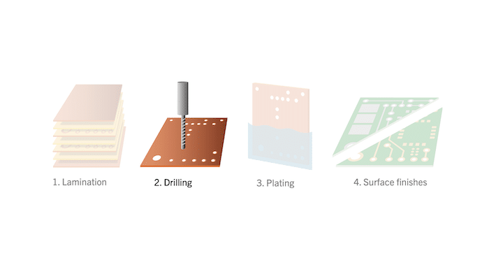
Drilling is an essential step in creating cavities in the board for various functions, including mounting components, creating vias, and establishing electrical connections between the various PCB layers.
Firstly, drilling creates connections through the PCB, allowing electrical signals to flow between the various layers. This function is crucial for multilayer PCBs, where connections between layers are essential.
Secondly, the position of the holes must be precise to guarantee correct operation of the printed circuit boards. This depends on both the machine used and the drilling parameters. Incorrect positioning can lead to assembly, connectivity, or operating problems.
Another crucial factor in the drilling process is hole diameter tolerance. In some cases, such as press-fit assemblies, the tolerance must be very strict to ensure correct assembly without damage to the board. Larger tolerances may be acceptable for other uses of the holes.
Hole quality is also important, as the roughness of the inner surface of the hole can affect copper deposition and thus electrical conductivity, material adhesion and even the durability of the final product. Holes with a reliability problem and/or poor quality can lead to bond failure problems.
Finally, the capacity of the drilling process determines the characteristics of the holes that can be produced. For example, mechanical drilling may be limited in terms of hole diameter and precision, while laser drilling offers greater flexibility for small diameters.
3. Choosing the right plating method
PCBs are used to electronically and mechanically connect electronic components using conductive tracks, etched pads made from copper foil laminated on a non-conductive substrate.
What is plating?
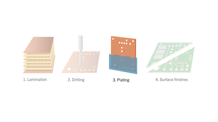
Plating is the process by which a thin layer of copper is deposited on the walls of the holes drilled in the PCB and on the conductors. This layer of copper creates electrical interconnections between the various layers of the PCB. Several methods can be used, such as electroplating or chemical plating.
Key points about plating:
- PTH (Plated Through Hole): Through-holes plating (PTH) is essential to create connections between the different PCB layers in the Z axis. This ensures that signals can flow freely between layers.
- Hole wall quality: The quality of the hole walls, including roughness and wicking, has an impact on the plating process. Well-metallized walls (with copper conforming to IPC-6012) are essential to ensure good electrical conductivity and increase vias reliability after component brazing and during use.
- Copper thickness: Copper thickness on hole walls is crucial for connections. For example, in thermal stress or thermal shock tests, insufficient copper thickness can lead to cracks, resulting in broken continuity and/or intermittent failures.
- Uniform copper thickness: Uniformity of copper thickness affects the tolerance of tracks and isolations, as well as the ability to create minimal tracks and isolations.
In short, plating plays a key role in the quality and reliability of printed circuit boards. Mastering the plating process is essential to guarantee optimum performance in your electronic applications.
4. The importance of surface finish for perfect solderability
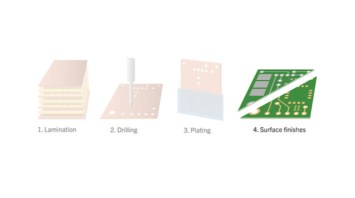
The surface finish of PCBs is a crucial step in protecting copper conductors from oxidation. It also ensures perfect solderability (IPC-610 compliant) when components are positioned and soldered on the board.
Key points concerning surface finishes:
- Assembly finish: The quality of the surface finish is essential for the assembly of components on the PCB. A well-treated (IPC-compliant) surface facilitates soldering and guarantees reliable solder joints.
- Process control: To achieve the right thickness of metal deposit or electroless plating, precise control of the finishing process is required. This ensures that pads and vias are finished to the required thickness for optimum brazing performance.
- Surface cleaning: Before finishing, the treated surface must be thoroughly deoxidized and cleaned to remove any contamination. Proper surface preparation ensures good adhesion of the metal or chemical deposit to the receiving surfaces.
Common surface finishes:
- Organic Solderability Preservative (OSP): OSP is a dipping or spraying process using an organic compound that selectively binds to copper, providing a protective organometallic layer. Although simple and inexpensive, OSP has limitations in terms of storage time and soldering phases.
- Hot Air Solder Leveling (HASL) with lead or lead free: This method involves selective deposition of tin/lead or tin/silver/copper (for HAL LF) by immersion in a bath of molten alloy, followed by levelling with hot air. HASL is robust but cannot be used for circuits with fine pitch components (<0.5 mm) or for HDI boards.
- Nickel/Gold (ENIG): ENIG uses a thin layer of gold on a layer of nickel. It offers good solderability and is suitable for a wide range of applications and virtually all soldering processes.
In short, surface finish is a key element in PCB quality, reliability, and performance. The choice of finishing method depends on your application specifications and performance requirements.
Beyond IPC
In the case of a printed circuit board with impedance requirements, the factory will document the track width/spacing, the impedance value of each layer, and then measure the impedance on the finished product. Other more standard elements we check include the cut-out of the printed circuit board and the diameter of the holes. In the report, the plan dimensions are defined and checked against actual results. The more complex the circuit, the more measurements are required.
For each batch, our factories test representative cards in accordance with IPC-TM-650 2.3.25 to ensure that the level of ionic contamination does not exceed 1.00µg / cm² in sodium chloride equivalent for HASL (leaded and lead free) and 0.80µg / cm² for non-HASL products. This exceeds IPC requirements. The final result is recorded in our certificate of conformity (for Asian factories only).
Finally, we know that some customers like to have a PCB sample that they can use as a reference for future evaluation or reference. The customer will receive a “solder sample” with a corresponding microsection (and impedance coupons if required by the customer).
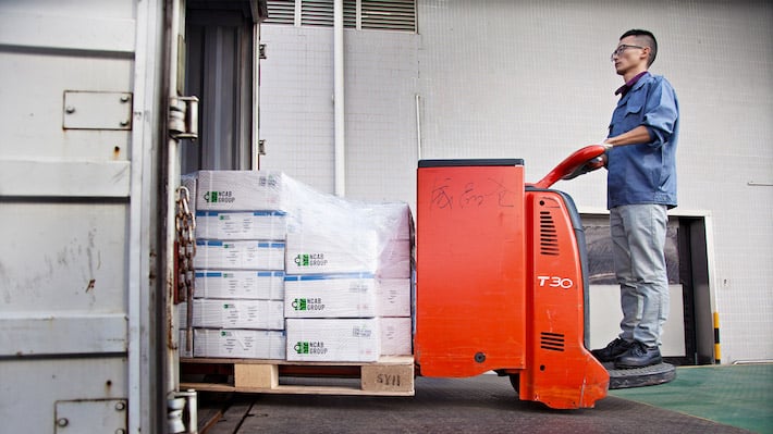
This document is enclosed with the NCAB box, sealed with blue tape at the top of the box as shown below.
In the railway sector, failure is not an option, especially for safety applications. The manufacture of a printed circuit board is a succession of mechanical operations and chemical processes. As already mentioned, certain processes have a direct influence on the PCB’s conformity and, above all, on its reliability over long periods of use, sometimes in harsh environments. It is for these and other reasons that our Factory Management carries out regular audits to ensure that these critical processes are under control, and to guarantee a high level of reliability.
Want to learn more about PCBs for the Railway Industry?
Read our blog post about requirements and standards that need to be considered when producing PCBs to the Railway Industry.
