Imagine you are a start-up company. You spent a year designing a product from start to finish. You have built the prototypes; there were some snags along the way but ultimately, the end product is perfect. You’re finally ready for volume production. Once you use multiple suppliers pricing out your bare board, you discover there’s a flaw in the design which will not allow the board to be produced for volume. Or at least not without paying a premium five times what you thought it would cost. Why? Because a via hole is .001 in (.025 mm) smaller than what can be achieved efficiently at many production factories. Because of the density of this design you cannot just increase the via size without reducing spacing beyond manufacturable limits in many areas. Your choices: start from scratch and redesign the board or pay the premium for specialty manufacturing. This situation could be debilitating for a company of any size, not just a start up.
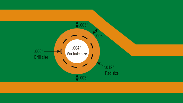
Let me back up here and explain this. There is this middle ground where some of the multilayer designs have the HDI attributes without going in as far as adding blind, buried, or microvias. So technically it’s still a multilayer, but it has features beyond the capabilities of most multilayer factories, and in many cases even beyond many offshore HDI Factories. The big problem we see is a level of density that demands a finished hole size below .006 in (.152 mm) or drill size below .00787 in (.2 mm) This represents the lower limit for mechanically drilling at most production factories offshore. Anything below that is beyond most factories’ capabilities.
NCAB and our prototype partner factories can mechanically drill down to .004 in which is .1 mm. Part of the reason for this lower limit is that the China factories, even HMLV, are set up for volume production. So when they drill the board they’re actually drilling a stack of production panels. They don’t want to drill a single panel at a time because it’s inefficient. US and EU “specialty” factories are not set up for volume production so they’re equipped and prepared to drill — albeit inefficiently — a single panel at a time.
When these examples pop up, it’s always an existing design and it’s almost always an existing design with a level of density that does not allow the via pad to support our minimum drill size. In the instance of vias, there is almost never something going into the barrel of the hole so that means the barrel of the hole is not a critical attribute of the design. Which means having the via at .005 in or .006 in or .007 in (.127, .152, .178 mm respectively) really has no impact on the finished board — it only helps achieve a greater density of the design. And if that’s part of a strict requirement, then fine. But in most instances, it is absolutely not necessary. The difference between .001-.002 in, if there is no space around the pads to support a larger finished hole size, a larger annular ring and a larger drill size, you could be easily quadrupling or greater the cost.

Talk to your PCB supplier regarding complex designs
Any time you have a layout with a via hole size smaller than .006 in (.152 mm), you should be talking to your board supplier before you finalize that data set. Because that is in the territory of being non-manufacturable with volume production at the lowest total cost.
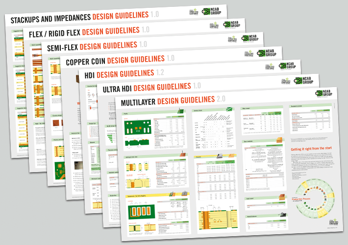
What I think may be happening here in some cases is the designer is using guidelines for a specific factory and the designer may not realize the guidelines are pushing the limits beyond industry averages. I do not advise this when going into advanced territory. NCAB created guidelines on averages throughout a cross-section of industry capabilities including dozens and dozens of various factories. The guidelines also clearly state when a feature is general, moderate or advanced. Using a tool like this puts you in a really good position. There is a high probability of the board being built efficiently. And also what if the board needs to be moved to another factory? Again, you will be in a very good position to effectively find another factory for the board without concern.
Bottom line is when you’re designing boards with advanced features, please always involve your PCB supplier as early as you can in the process to get it right from the start. A simple and small adjustment in the design can make all the difference.

PCB design guidelines
Get it right from the start with our PCB design guidelines. To prevent getting it wrong from the start, we have put together our design guidelines, to use as a checklist.
