Heavy copper PCBs

What is a heavy copper PCB?
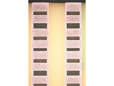
It is a PCB made with two or more conductive foils which has a conductive copper layer thickness of 3oz or more. When space is limited and it’s not possible to carry high currents by widen the track, the use of heavy copper PCB can effectively increase the current-carrying capacity of the circuit while supporting great heat dissipation.
Typical Track and Gap capabilities by copper thickness
| Base Copper | Capability (mm) | |
| Inner Layer Track / Gap | 102.9µm (3OZ) | 0.20/0.20 |
| 137.2µm (4OZ) | 0.25/0.25 | |
| 171.5µm (5OZ) | 0.35/0.35 | |
| 205.7µm (6OZ) | 0.40/0.40 | |
| Outer layer Track / Gap | 102.9µm (3OZ) | 0.25/0.30 |
| 137.2µm (4OZ) | 0.30/0.30 | |
| 171.5µm (5OZ) | 0.40/0.40 | |
| 205.7µm (6OZ) | 0.45/0.50 |
High current carrying
We support the production of heavy copper PCBs for high-power applications such as EV-chargers, high current systems, power storage systems, and base stations. Our typical capabilities include copper thicknesses over 3oz and track/gap designs such as 8/8 mils. For requirements beyond 6oz, please contact us to discuss feasibility and factory availability.
Efficient heat dissipation
The thermal conductivity efficiency of ultra-heavy copper foil is significantly enhanced, which reduce the operating temperature of components, extend equipment life and improve system stability.
High mechanical strength and reliability
Heavy copper greatly enhances the PCB’s ability to resist impact and deformation, and is suitable for long-term stable operation in industrial automation and harsh environments.

Download our PCB design guidelines to get your PCBs right from start

Contact us
Please contact us if you need further information or assistance, we are happy to help you.
