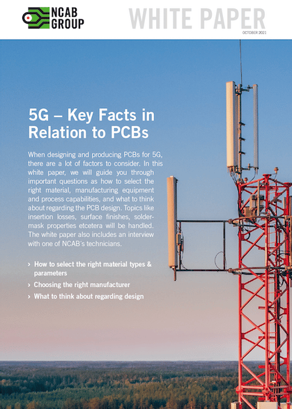
When designing and producing PCBs for 5G, there are a lot of factors to consider. In this white paper about 5G PCBs, we will guide you through important questions as how to select the right material, manufacturing equipment and process capabilities, and what to think about regarding the PCB design. Topics like insertion losses, surface finishes, soldermask properties etcetera will be handled.

5G – Key Facts in Relation to PCBs
Download this white paper about 5G PCBS and learn about:
- How to select the right material types & parameters – learn about insertion losses, dielectric losses, conductor losses, glass weave style, solder mask properties and surface finishes.
- Choosing the right manufacturer – learn about why the the manufacturer’s equipment and process capabilities are critical.
- What to think about regarding design – learn about thermal management, power integrity, signal integrity and get design tips about stack up & interconnect, back drilling and annular ring.
The white paper also includes an interview with two PCB experts; Ellefen Jiang, PCB design manager, and Barry Fang, FAE manager at NCAB Group about design and manufacturing of 5G PCBs.
Sending... Please wait as this can take a while...
Access our Whitepapers
To access Whitepapers, please complete the short form below.
You will receive a link to the download page by e-mail - please check your spam folder if you do not receive it.
Your contact information will be saved and will be used to send a link to the page where you can download the whitepaper. The email address you have provided may be used to send you information we think you may find interesting. Your contact information will only be used by NCAB Group. By clicking on “Send” you will be agreeing to this. For further information about how NCAB processes your personal information, please see our Privacy Policy.
