What is important to consider regarding PCB design for extreme environments? Learn more about the challenges and how the PCBs needs to be adapted for thermal management, altitude and shock and vibration events.

In part one of this blog series I talked more about applications and challenges PCBs face in harsh and extreme environments. This time I want to dive deeper into PCB design considerations regarding PCB design for extreme environments. Designing a PCB for a non-demanding environment can be a daunting task in itself. There are many considerations to make, and some will change depending on other decisions made. When I think about some of the challenges unique to extreme environments, I am amazed at the robust technology. The negative effects of altitude, vibration, shock, and heat plagues electronics systems we rely on every day.
Change in altitude – how does it effect the PCB
One challenge many PCB designers have to resolve is the effects of air density with the change in altitude. Without going into too much detail, the density of the atmosphere becomes lighter as altitude increases. There is a region in the atmosphere between the lower atmosphere and the vacuum of space where electricity can arc at lower voltages. What this really equates to is the breakdown voltage of the air in the thinner atmosphere is smaller. This allows electricity to arc across conductors at lower voltages than at sea level. To make matters worse, charge builds up quicker at a point than it does when compared to a rounder surface. The charges that build up can potentially act as arc points.
There are some things we can do to mitigate this challenge. First, consult IPC-2221, Section 6. This part of the Designer’s Specification has the “good stuff” in regard to calculating how much electrical clearance your design will need. Another way we can add mitigation to keep arcing at bay is to round out the corners in our design. By that I mean eliminate the ninety degrees inside and outside corners on plane pours, on surface mount pads, and the bends of traces. Engineers can also look at connection pins. Since these areas of the board are often associated with different voltage levels there is more of a risk for arcing at these places as well. Sometimes we have unused pins on the connector that will allow us even greater clearance if we use every other pin.
What can happen when the PCB is exposed to extreme shock and vibrations?
Some environments subject PCBs to extreme shock and vibration events. Extreme shock events are events that subject the PCBs to a high amplitude of movement force, for a short duration of time. Whereas extreme vibration events subject PCBs to longer periods of movement with less amplitude. The movement force causes the board to oscillate about the center of mass. In turn, the oscillations stress the PCB materials and connection points. The materials will be stressed at the point where the pre-preg bonds with the copper. The hole barrels are internal connection points that could possibly crack, causing intermittent operation at best. There are many small things we can do to mitigate shock and vibration. The key is to find the minimum amount of mass to add to the system while maintaining mechanical stability. Along with staking and potting compounds, below are some PCB design considerations.
PCB design for handling shock and vibrations
We can design more mounting holes into the board. More mounting holes means more mounting points to the chassis and more stability. This will also allow the addition of more dampening devices to be mounted into the system.
Another aspect of the PCB we want to address is the stackup. In class, I had practical assignments like designing a board and stackup for a satellite application. This was my favorite assignment. For boards that will be subject to extreme shock or vibration events it is critical to ensure the pre-preg has enough resin content to withstand these types of events. The pre-preg resin is the glue that holds the board together. During shock and vibration events the PCB may flex and cause stress on the connection points. In order to mitigate as much stress as possible we should consider using pre-pregs with over 50% resin content. In addition, adding more than two sheets is another way to add more bonding strength. I say this as a consideration because signal integrity requirements do not always allow changing dielectrics easily. What if you do not have a signal integrity requirement? If three sheets of pre-preg is good then four has to be better, right? It may. At a certain point too much pre-preg will be detrimental to the layer-to-layer registration. I would try to stay with three sheets max, unless your PCB vendor says otherwise. If you are after more thickness, but cannot add any more pre-preg, consider using unclad cores in the stackup. Unlike the pre-preg, an unclad core is already cured, so it does not add any resin to the press cycle. Thus, layer-to-layer registration is not sacrificed.
Finally, I want to talk about the internal connection points. As the PCB oscillates, the hole barrels are also oscillating. This stresses the plating in the holes. As the plating is stressed it can crack. Some PCBs may work again after they are brought up to operating temperature, and some may experience catastrophic failure. Either way, it is not always possible to retrieve said PCB in the field. Adding extra plating to the holes is just one more consideration to having a robust PCB. It will not work for every application.
Thermal management and PCBs
Thermal management is the last challenge I want to discuss. For a non-demanding application PCB, passive cooling, such as convection, will be an adequate thermal management solution. Other PCBs may be connected to the chassis for heat transfer, and some may be cooled by other devices. PCBs that operate in extreme environments cannot always be cooled by these methods. We can design the PCB to have active cooling solutions.
An easy way to add heat mitigation is to simply increase the copper thickness of the PCB. Simply stated, thicker copper dissipates heat better. As a word of caution, make sure the electrical space in the PCB data will support manufacturing the PCB with thicker copper. Your PCB vendor will know how much space you will need for sure, so they are always a good source for this type of information.

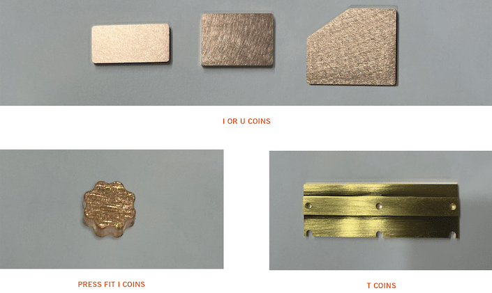
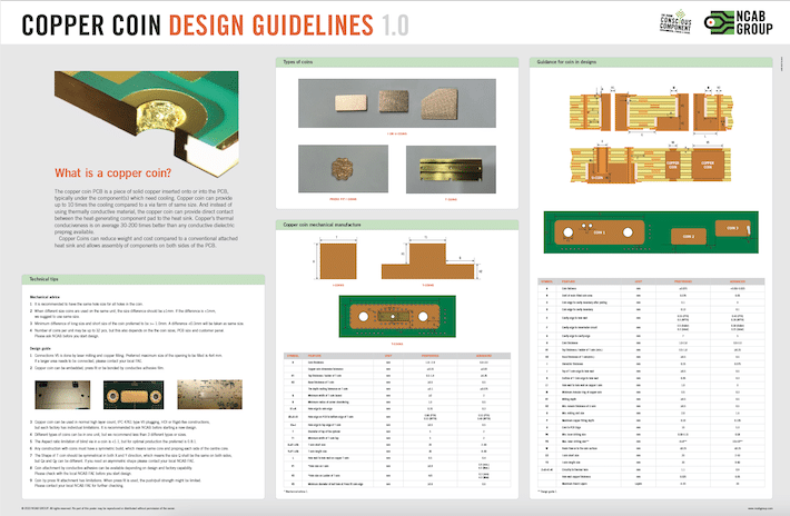
If simply increasing the thickness of the copper does not alleviate the thermal management issues, there is an option to add copper coin technology to the PCB. The easiest way to describe this technology is it is like building a discreet heat sink into the PCB. It is positioned directly under the component so it is in contact with the component. In some cases, the coin can be electrically connected to the component. The advantage here is greater heat transfer rather than simply increasing the copper thickness. One of the disadvantages is the number of copper coins that can be placed on one panel. This amount will vary from manufacturer to manufacturer, but a consideration which should be remembered regardless of the manufacturer; every time a coin is inserted into a PCB a weak spot is created in the PCB material. Too many weak spots can cause warpage and unintended consequences. Consider an environment with shock and vibration events with many coins in one design.

Instead of designing the PCB with too many copper coins, consider metal core construction. Metal cores can be pressed into the stackup or pressed onto a layer in order to provide the ultimate in heat sinking ability. When planning for metal cores, dielectric thicknesses should be carefully considered. We want to use the thinnest dielectric possible between the component layer and the metal core. This is because thinner dielectrics have less heat resistance. This advice goes directly against the recommendation I made for designing stackup to resist shock and vibration events. As the PCB gets more complex we must consider each moving part of the “machine” in relation to other parts.
Extreme environments subject PCBs to many new hazards we must consider, while other challenges will amplify in magnitude. It is difficult, at best, to learn everything we can in order to mitigate the effects extreme environments have on our PCBs. Hopefully, adding a little here and a little more there will help you design a more robust PCB. The best advice I can provide is to always work with your PCB supplier as early as possible in the design phase – they know both the design considerations and manufacturing capabilities to help design the PCB in the most efficient and sustainable way.
