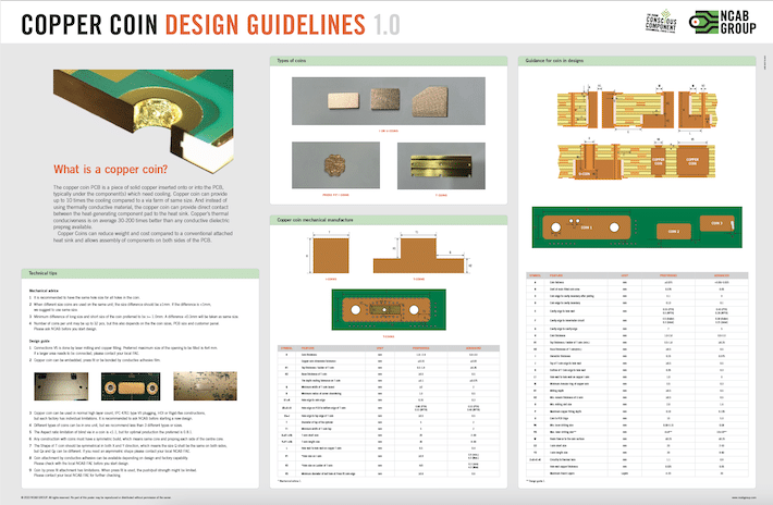
A copper coin is a multilayer PCB but with the addition of a solid piece of copper, called a coin, embedded into the PCB’s stack-up. This allows a direct thermal connection from one side to the other or from a specific layer to an outer layer. Learn more in the video.

Design guidelines for copper coin
Nothing affects the PCB’s total cost and reliability as much as the initial design. That is why we have put together our PCB design tools for engineers, designers and anyone else involved in the PCB design or production process.
Design guidelines for Multilayer PCB, HDI PCB, Ultra HDI PCB, Flex / Rigid-Flex PCBs, Semi-Flex PCB, Copper coin and Stackups and Impedances are available for download.
Learn more about copper coin
Copper coin PCBs – efficiency and reliability in thermal PCB management
The overall goal of thermal management at the bare board and assembly level is to move the heat away from the heat-generating components to an external heat sink for dissipation. Better heat transfer will usually translate to lower mean time between failures (MTBF) and at times will be a deciding factor at meeting product design specifications.
In this blog post we want to dive deeper into the growing technology of Copper Coin PCBs. Heat transfer occurs at a higher rate when materials of high thermal conductivity are used. Copper is extremely conductive offering upwards of 400 W/mK, as is for example other materials like diamonds, which can be up to five times more thermal conductive than copper. But, who wants to use diamonds in their PCBs? Copper is one of the best ways to manage heat while keeping electrical and or thermal conductivity.
