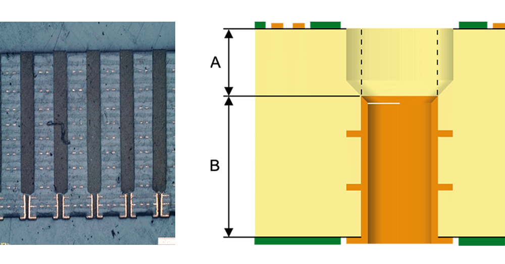
For high frequency applications we need to prevent signal loss and therefore when one layer is connected to another and the signal travels from one layer to another it must pass through a via hole that connects the layers. If the signal is to pass layer one to layer two in a 20 layer board, for example, then part of the via structure is considered as ‘excess’ and for this application it is best to remove the excess copper from this hole as it acts as an antenna and impacts the signal.
We use back-drilling (controlled depth in z-axis) to drill out the ‘excess’ copper in the hole in order to get better signal stability. Ideally the shorter the stub (‘excess’ copper) then the better the result. Back-drill size should be typically 0.2mm larger than corresponding via.

| BACK DRILLING / COUNTER BORE (mm) | |||
|---|---|---|---|
| A: Depth tolerance | +/-0.20 | +/-0.15 | +/-0.10 |
| B: Min. remain thickness and tolerance | 0.5+/-0.25 | 0.35+/-0.1 | 0.3+/-0.1 |
