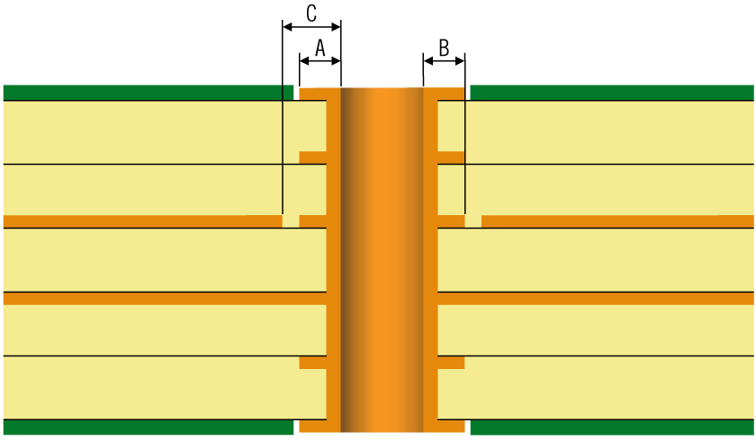
This varies from manufacturer to manufacturer, but in general you can say that the majority of manufacturers can produce them as follows:
A = 0.15 mm
B = 0.20 mm
C = 0.30 mm

This varies from manufacturer to manufacturer, but in general you can say that the majority of manufacturers can produce them as follows:
A = 0.15 mm
B = 0.20 mm
C = 0.30 mm
