What is thermal resistance?
In this video you can learn about thermal resistance and thermal conductivity.
What does “UL marking” mean?
Security is keyin the electronics industry. It is vital that users can rely on the finished product when considering factors such as fireand electrical safety, which means that both the PCB and the materials theycontain must measure up to the highest standards. To ensure that the boards doconform, it has become common practice to UL certify the constituent materialsor the PCB itself.
To start with, what is UL? The letters UL stand for Underwriters Laboratories.
Why is UL recognition important? UL is a major authority and enjoys a good reputation in the PCB industry. The company is irreplaceable for testing fire and electrical safety. Customers from around the world – including well-known Chinese companies – demand factories that can achieve UL recognition. Having UL recognition is therefore very important for PCB factories to produce secure boards and be able to access the international market.
What is back-drilling technology?
For high frequency applications we need to prevent signal loss and therefore when one layer is connected to another and the signal travels from one layer to another it must pass through a via hole that connects the layers. If the signal is to pass layer one to layer two in a 20 layer board, for example, then part of the via structure is considered as ‘excess’ and for this application it is best to remove the excess copper from this hole as it acts as an antenna and impacts the signal.
We use back-drilling (controlled depth in z-axis) to drill out the ‘excess’ copper in the hole in order to get better signal stability. Ideally the shorter the stub (‘excess’ copper) then the better the result. Back-drill size should be typically 0.2mm larger than corresponding via.
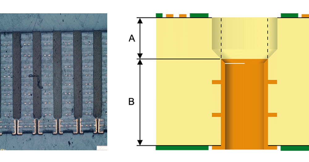
| BACK DRILLING / COUNTER BORE (mm) | |||
|---|---|---|---|
| A: Depth tolerance | +/-0.20 | +/-0.15 | +/-0.10 |
| B: Min. remain thickness and tolerance | 0.5+/-0.25 | 0.35+/-0.1 | 0.3+/-0.1 |
Should approval for addition of teardrops be added in the procurement documentation?
According to new IPC-6012D section 3.4.2 it is allowed to add teardrops to the tracking when boards shall comply to classes 1 & 2.

If you do not want tear-drops, highlight that in the procurement documentation. But add enough annular ring.
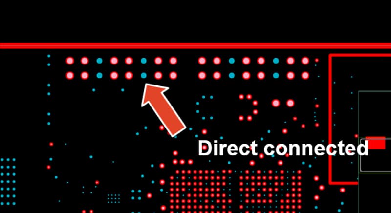
What is meant by a thermal pad?
For SMD components, especially the smaller ones, use thermal relief pads to simulate the same thermal mass on both terminations to avoid tombstoning, twisted components or even in worst case broken components.
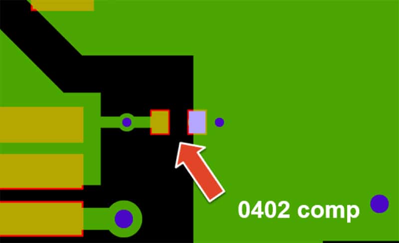
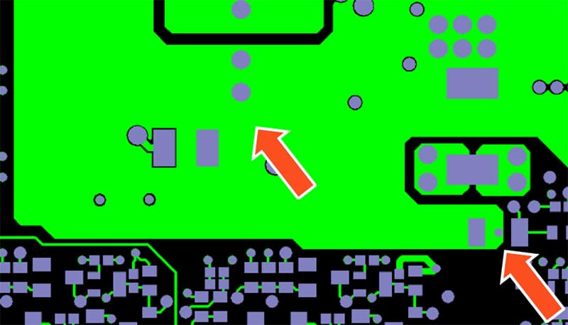
For hole mounted (HMD) components we use thermal relief pads on inner layer planes to help wetting in the hole barrel. Formulas for thermal relief pads can be found in IPC-2220 series.
Is there more than one type of controlled impedance?
Yes, there isand these are explained below:
Differential impedance – Impedance of a pair of conductors with equal and opposite polarity signals – same amplitudein anti-phase with each other.
Odd mode impedance – Impedance of one side of a pair of conductors which both have equal and opposite polarity signals – same amplitude and anti-phase.
Even mode impedance – Impedance of one side of a pair of conductors which have equal signals – same amplitude and same polarity.
Common mode impedance – Impedance of a pair of conductors which have equal signs – same amplitude and same polarity.
Learn more about impedance
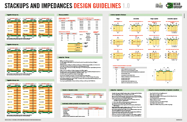
Design guidelines for stackups and impedances
Download our PCB design guidelines for Stackups and Impedances to get your design right from start.
What is controlled impedance?
Consider the PCB signal as it travels along a track controlling impedance means that we control the performance or speed of that signal at a point along a track. Related to resistance, capacitance and conductance of the track in question. The impedance is also measured in Ohms, it is different than resistance which is a DC characteristic. Impedance is an AC characteristic, meaning that it is related to frequency.

Design guidelines for stackups and impedances
Download our PCB design guidelines for Stackups and Impedances to get your design right from start.
What is a copper coin PCB?
A copper coin is a multilayer PCB but with the addition of a solid piece of copper, called a coin, embedded into the PCB’s stack-up. This allows a direct thermal connection from one side to the other or from a specific layer to an outer layer. Learn more in the video.
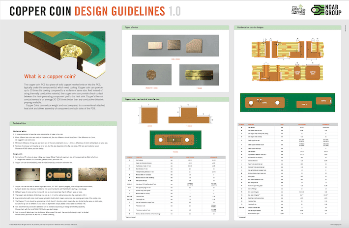
Design guidelines for copper coin
Nothing affects the PCB’s total cost and reliability as much as the initial design. That is why we have put together our PCB design tools for engineers, designers and anyone else involved in the PCB design or production process.
Design guidelines for Multilayer PCB, HDI PCB, Ultra HDI PCB, Flex / Rigid-Flex PCBs, Semi-Flex PCB, Copper coin and Stackups and Impedances are available for download.
Learn more about copper coin
Copper coin PCBs – efficiency and reliability in thermal PCB management
The overall goal of thermal management at the bare board and assembly level is to move the heat away from the heat-generating components to an external heat sink for dissipation. Better heat transfer will usually translate to lower mean time between failures (MTBF) and at times will be a deciding factor at meeting product design specifications.
In this blog post we want to dive deeper into the growing technology of Copper Coin PCBs. Heat transfer occurs at a higher rate when materials of high thermal conductivity are used. Copper is extremely conductive offering upwards of 400 W/mK, as is for example other materials like diamonds, which can be up to five times more thermal conductive than copper. But, who wants to use diamonds in their PCBs? Copper is one of the best ways to manage heat while keeping electrical and or thermal conductivity.
What is copper wrap?
Copper wrap is a continuous deposit of plated copper that is deposited within the barrel of the hole and extends onto the surface of the PCB (or the surface of the innerlayer core if part of a HDI structure) by a minimum of 25 um.
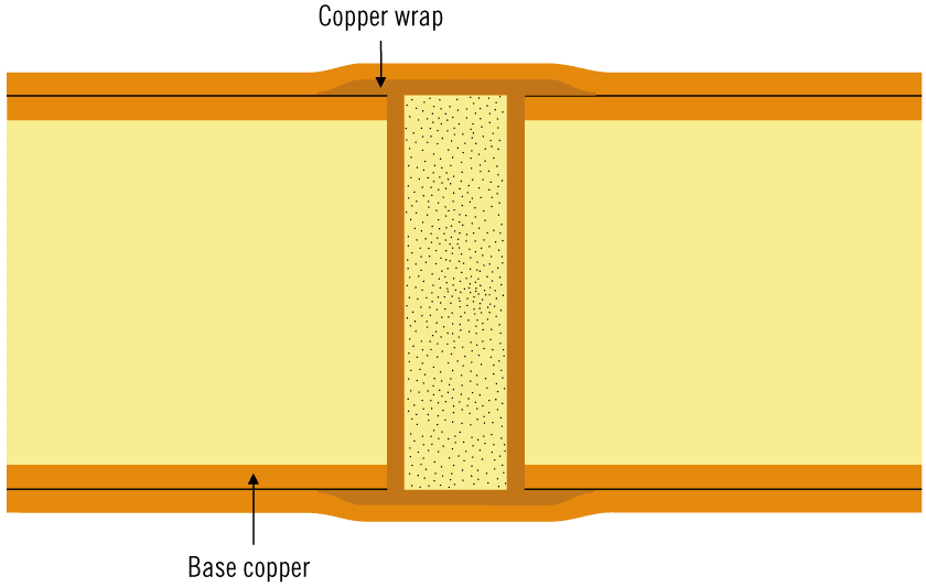
For class 2 demands the thickness of the surface deposit of the copper wrap is minimum 5um, but for class 3 demands this will vary dependant upon where this feature is situated within the build. Please consult our technicians for further information on class 3 demands.
What is the “aspect ratio”?
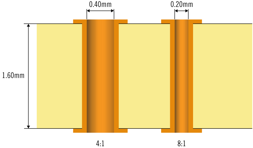
The relationship between the diameter of the hole and its length. When a manufacturer states that their production has an “aspect ratio” of 8:1 it means, for example, that the hole’s diameter is 0.20 mm in a 1.60 mm thick PCB.
For HDI structures, the aspect ratio for microvia is limited to 1:1, but 0.7-0.8:1 is preferable to easy the plating.
