Skip to content
NCAB Group

NCAB Group

  • About us
    • About us
      • Organization
      • Vision
      • Values
      • Key figures
      • History
      • Policies
      • Privacy Statement
      • Newsroom
      • News
      • PCB Blog
      • Webinars
      • Terms and conditions of sales and delivery
      • Downloads
  • What we do
    • What we do
      • Benefits of working with us
      • Our approach to reliable PCBs
        • Getting it right from the start
        • Prototyping for volume production
        • Maximizing PCB factory performance
        • Keeping deliveries on time
      • PCB portfolio
        • Multilayer PCBs
        • HDI
        • RF – Radio Frequency
        • IMS – Insulated Metal Base
        • Flexible
        • Rigid-Flex
        • Semi-Flex
        • Double sided
        • Heavy copper PCBs
      • Industries we serve
        • Aerospace
        • Automotive
        • Datacom
        • Defense
        • Industrial
        • Medical
        • Power/energy
        • Railway
        • Safety critical
        • Telecom
      • Our customers
  • Sustainable business
    • Sustainable business
      • Sustainability strategy
        • Supply chain
        • Employees
        • Customers
      • FAQ about sustainability
      • Environmental roadmap
      • Downloads
  • PCB Technology
    • PCB Technology
      • PCB portfolio
        • Multilayer
        • HDI
        • RF – Radio Frequency
        • IMS – Insulated Metal Base
        • Flexible
        • Rigid-Flex
        • Semi-Flex
        • Double sided
        • Heavy copper PCBs
      • Capability roadmap
      • PCB Specification
      • PCB design
      • PCB design tools
        • PCB design guidelines
        • PCB design tips
        • PCB design checklist
        • PCB cost drivers
      • Surface finishes
      • Webinars
      • Base materials
      • Microvias
      • FAQ about PCBs
      • NCAB Group Lab
      • Production process
      • Downloads
  • Career
  • Investors
  • Contact
    • Contact
      • Head office
      • Factory Management
      • Europe
      • Austria
      • Belgium
      • Bulgaria
      • Czech Republic
      • Denmark
      • Finland
      • France
      • Germany
      • Hungary
      • Italy
      • Netherlands
      • North Macedonia
      • Norway
      • Poland
      • Portugal
      • Romania
      • Serbia
      • Slovakia
      • Slovenia
      • Spain
      • Sweden
      • Switzerland
      • Turkey
      • United Kingdom
      • North America
      • Canada
      • USA
      • Asia
      • China
      • Malaysia
      • Can´t find your country?
  • Choose language
    • Deutsch
    • Dutch
    • English
    • Español
    • Français
    • Italiano
    • Polski
    • Suomi
    • Svenska
    • 中文

Tag: HDI

2022 11 21 | Blog

Ultra HDI PCBs put high demands on technology and manufacturing

Ultra HDI printed circuit boards are extremely dense boards with conductor width and isolation distance and dielectric thickness of less than 50 µm. Read more here.
2021 05 31 | Blog

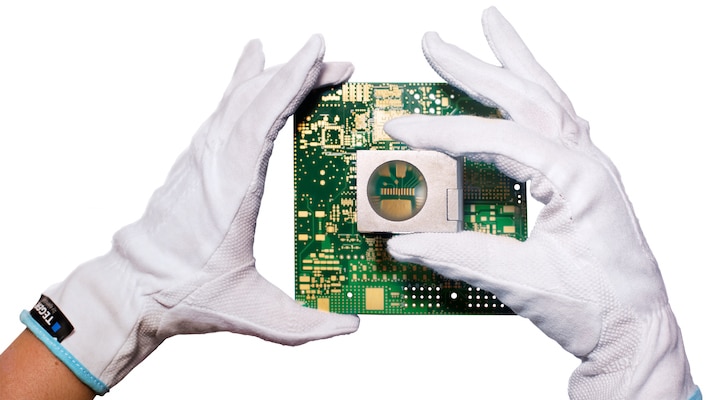
HDI – high density interconnect PCBs – design trends

With a higher wiring density per unit area than conventional PCBs, HDIs require different designs. Here you can read about HDI PCB designs & trends.

2015 02 24 | Blog

More design tips – get it right from the start

  COMMON DESIGN PROBLEMS REGARDING HDI PRODUCTION PROBLEMS DEPENDING ON THIS BEST SOLUTION Too tight demands on the thickness of overplating of plugged vias. (POFV or VIPPO) Affects the flow of the process, at a reasonable thickness of the overplating all the vias can be drilled in the same operation, which makes the process much […]

2014 10 06 | Blog

High-tech PCBs – design tips to get it right from the start

In issue no 3 of In Focus – NCAB Group´s newsletter, we dig deeper into high-tech PCBs. As an appetizer, we will already now give you some useful designtips regarding HDIs. COMMON DESIGN PROBLEMS REGARDING HDI PRODUCTION PROBLEMS DEPENDING ON THIS BEST SOLUTION Dielectric too thick for laser vias Increased time for laser drilling, lower […]

Back to top
  • About us
      • Organization
      • Vision
      • Values
      • Key figures
      • History
      • Policies
      • Privacy Statement
      • Newsroom
      • News
      • PCB Blog
      • Webinars
      • Terms and conditions of sales and delivery
      • Downloads
  • What we do
      • Benefits of working with us
      • Our approach to reliable PCBs
      • PCB portfolio
      • Industries we serve
      • Our customers
  • Sustainable business
      • Sustainability strategy
      • FAQ about sustainability
      • Environmental roadmap
      • Downloads
  • PCB Technology
      • PCB portfolio
      • Capability roadmap
      • PCB Specification
      • PCB design
      • PCB design tools
      • Surface finishes
      • Webinars
      • Base materials
      • Microvias
      • FAQ about PCBs
      • NCAB Group Lab
      • Production process
      • Downloads
  • Career
  • Investors
  • Contact

Contact us

    • Head office
    • Factory Management
    • Europe
    • Austria
    • Belgium
    • Bulgaria
    • Czech Republic
    • Denmark
    • Finland
    • France
    • Germany
    • Hungary
    • Italy
    • Netherlands
    • North Macedonia
    • Norway
    • Poland
    • Portugal
    • Romania
    • Serbia
    • Slovakia
    • Slovenia
    • Spain
    • Sweden
    • Switzerland
    • Turkey
    • United Kingdom
    • North America
    • Canada
    • USA
    • Asia
    • China
    • Malaysia
    • Can´t find your country?

© 2011-2025 NCAB GROUP CORPORATION

Follow us here

  • Read our Blog
  • Follow us on Facebook
  • Visit our Youtube page
  • Visit our LinkedIn page
  • Follow us on Instagram