Driven by electricity instead of fossil fuels, electric vehicles (EVs) are revolutionising and shaping our mode of transportation. But what are electric vehicles and their reduced environmental impact if you’re not able to charge them? Learn about PCBs for electric vehicle charging – the trends, design considerations and NCAB´s added value.

Printed Circuit Boards (PCBs) are crucial components in EVC systems, playing a pivotal role in ensuring the reliability, efficiency, and safety of the charging infrastructure. From managing power distribution to contributing to the infrastructure of the design, PCBs are vital in ensuring reliable and high-power charging capabilities. And in this guide, we will not only highlight the pivotal role of EVC PCBs, but also discuss current trends, how to design PCBs for EVC, the different types of EVC, and the added value that we as a company provide our customers.
Current trends in the electric vehicle PCB Industry
The miniaturisation trend in EVC, especially Level 2 chargers
With a fast-growing industry and huge leaps in technological advancements, EVCs have not only become more complex, but their size and design have changed too – becoming not only more compact but even lighter. And as EVCs evolve, we too need to develop and evolve our PCB technology and designs as well. With more complex and smaller sized EVCs being made, we’ve needed to find ways to use the limited space which is provided. This in turn means:
- Higher density of circuit board and more layers through the PCB – this provides more circuitry for function and is necessary to support electronic product development
- Thinner materials (PP/CCL)
- Less space for connectors and 3D installs
- PTH is not enough, so we therefore need laser drilled microvias and buried via’s that are smaller and connect selected layers rather than going through the whole PCB. This in turn increases number of interconnections
- Smaller components and smaller features.
Overall, with increasingly complex products that are following the trend of miniaturisation, we too need to follow the trend which means greater demands on the factories.
High-speed charging
Another noticeable trend in EVC relates to the speed that the vehicle is being charged. With increasing demand for faster charging times, PCB technology is also evolving to support efficient and reliable high power charging operations.
PCBs used in high-speed charging systems need to handle higher currents and voltages. This includes, along with other considerations, using certain material choices, and a great deal of copper to both conduct the current and dissipate excess heat. The design of the high-speed charging PCBs is another factor that should be taken into consideration.
For example, ensuring that the conductor width and insulation distance are properly positioned.
Integration with Renewable Energy
Following the path of sustainability and reducing the carbon footprint associated with electric vehicles, integrating the EVC system with renewable energy sources such as solar panels, wind power, as well as power grid, is another trend within EVC. For instance, you can install solar panels on your own property to store energy in a battery pack, which can later be used when electricity prices are high.
Enhanced user-friendly interfaces
A notable technological advancement within EV is the integration of user-friendly interfaces aimed at improving the charging experience. These interfaces encompass features such as touchscreens, mobile apps, RFID card readers, and intuitive controls, all designed to enhance user convenience and overall experience during the charging process.
Key factors to consider when designing and producing a PCB for electric vehicle chargers
By working collaboratively with our technicians and our factories, we can make positive impacts in the following areas:
PCB Design
EV charging is an application and end-product which requires high-power circuit design.
High-power circuits are characterized by their significantly greater voltage or current levels compared to those utilized in low-power circuits. Designers bear the responsibility of ensuring the circuit functions within the appropriate voltage and current parameters, while also incorporating adequate cooling and safety measures.
When it comes to high-power PCBs, they typically follow one of two design approaches: layout design or reference design. Layout design pertains to the arrangement of components on the PCB, while reference designs are typically created with specific layouts in consideration. The PCB layout must be meticulously crafted to accommodate high-power components effectively and minimize the generation of noise.
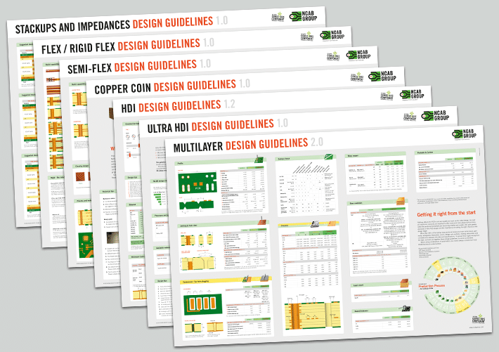
Another consideration to consider is component placement. The high-power component placement is a design technique that is used to reduce the thermal resistance of the PCB. This technique is used when there are high-power components on the PCB. For more advice about PCB design, you can contact your local contact, or download our free PCB design guidelines.

PCB design guidelines
Get it right from the start with our PCB design guidelines. To prevent getting it wrong from the start, we have put together our design guidelines, to use as a checklist.
Solder mask thickness
The solder mask and its thickness are another important aspect to consider in the high-power design of EVCs.
Heavy copper on external layers could lead to the use of higher solder mask thickness (in order to cover the “gap” between the tracks). Factory could apply double solder mask deposit. The solder mask thickness is important, and the designer should also check the datasheet of solder mask used (for example: the dielectric strength, the surface resistance). The IPC recommendations for solder mask are included in IPC-SM-840. By default, the IPC suggests using Class T for performance class 2 circuits and Class H for performance class 3 circuits. The solder mask should not be considered as the “single insulating”. Furthermore, the designer should also consider a conformal coating.
Power copper (Cu) weights – Lower Cu weights
Power copper (Cu) weights refer to the thickness or amount of copper used for power traces on a PCB. In electric vehicle chargers, power copper weights play a crucial role in enabling efficient and reliable power transmission.
Copper is a very good conductor of heat (385 W/mK) and not only does a heavier copper thickness offer a greater current carrying capacity, it also allows more heat to be dissipated.
However, we must also think of more than just the thickness of copper on the surface. Of course, a thicker deposit is key for thermal management, but we must consider the width of the track or copper feature as this will act to increase the cross-sectional area, thus increasing the amount of heat that can be dissipated through the copper track. Heavier copper also limits the ability to have finer features on the circuitry. However, there is a solution if the design requires small features or components.
Trace width and thickness
The thickness of the copper traces is determined by the power that will be applied to them. The higher the power, the thicker the trace needs to be.
Designers should consider the copper foil thickness and follow the minimum track and gap according to the copper thickness selected (this is important to check if the tracks will be designed on internal or external layers). The thicker copper thickness you need, the thicker trace you must follow. For example, if you need to use 3oz: 105µm copper thickness (external layers), the minimum trace width will have to be >350µm on external layer, as general factory.
Did you know?
The size and layer count of the PCB can have a major impact on sustainability? If we can reduce the size of the PCB then we can also minimize the amount of materials used, resulting in reduced waste and environmental impact.
Material properties
To be able to reduce isolation distance between copper traces / copper areas, material with better CTI (Comparative Tracking Index) properties can be considered.
Standard FR4.0 & FR4.1 will normally meet PLC 3 (See table below). Better material can be used which are able to meet both PLC 1 & PLC 0. Factors such as availability, lead-time, and UL approvals need to be taken into account. Please contact your local NCAB engineer for more comprehensive information.
| Tracking Index (V) | PLC |
|---|---|
| 600 and Greater | 0 |
| 400 through 599 | 1 |
| 250 through 399 | 2 |
| 175 through 249 | 3 |
| 100 through 174 | 4 |
| < 100 | 5 |
Materials with high Maximum Operating Temperature (MOT) can also be considered if the temperature inside the enclosure or on boards surface will be high. PCB made from FR4.0 and FR4.1 can be approved from UL with a maximum of 130°C in MOT, but boards made FR15.0 and FR15.1 can be approved to a minimum 150°C.
Thermal management
With components and increased power demand being two main causes of heat, thermal management is vital to reliable designs of EV chargers, as excessive temperature can contribute to failures. Thermal management relates to the methods employed to transfer excess heat from one location to another. In the case of EVCs and the PCB, our focus is to transfer the excess heat away from the component, dissipating the heat either into or through the PCB from one side to another.
There are a few solutions to this, one being layout:
- Place heat generating components away from the board edge to help dissipate the heat evenly.
- Do not group heat generating components together, but instead spread them out.
- Keep heat generating components away from smaller more sensitive components.
- Consider heat sinks early in the process.
- Optimise enclosure airflow of the assembled unit.
- Allow for wider tracks to conduct heat away and use heavy copper foils on the inner layers. Keep in mind however that with high copper weights, space can be an issue.
AC chargers & DC chargers – two types of EV charging systems
AC (Alternating Current) and DC (Direct Current) chargers are two types of charging systems used for electric vehicles.
What are some few differences between AC and a DC charge?
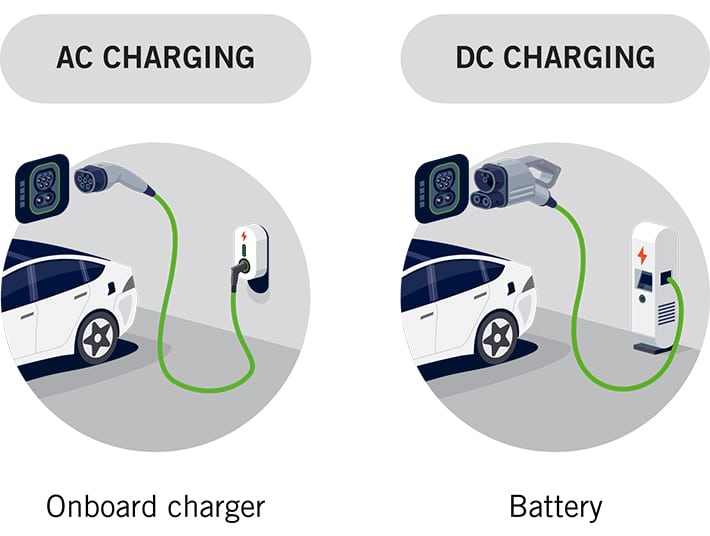
- AC charging and DC charging can be distinguished by the location of power conversion. Unlike AC chargers, which convert AC power inside the vehicle using the onboard charger, DC chargers have the converter integrated within the charger unit. As a result, DC chargers can supply power directly to the car’s battery without relying on the onboard charger for conversion.
- AC chargers are specifically designed to operate with alternating current, the type of electricity typically provided by power grids. In contrast, DC chargers are tailored to function with direct current, which is commonly stored in batteries or generated by solar panels.
- AC chargers are commonly found in various locations such as homes, workplaces, parking lots, and public charging stations. Whilst DC chargers are typically found in public charging stations along highways, major routes, and urban areas, catering to long-distance travel and quick top-ups.
- DC is used for fast charging, whilst AC chargers offer lower power levels resulting in longer charging times.
- AC chargers typically offer charging speeds ranging from 3.7 kW to 22 kW, depending on the specific charger and the EV’s onboard charger capacity. DC chargers can provide high-power charging rates ranging from 50 kW to several hundred kilowatts, enabling rapid charging and reducing the time needed to recharge an EV’s battery.
- Generally, DC use higher voltage – DC chargers are increasingly adopting higher voltage levels to enable faster charging. The use of higher voltages, such as 400V, 800V, or higher, reduces charging time by allowing higher currents to flow into the EV battery. Higher voltage charging also results in reduced losses and more efficient power transfer.
It is worth noting here that new investigations have shown that high voltages in a PCB can create severe damages over time; this is when the PCB itself has traces with voltages above 500V.
Within EV charging, the performance of large current and high voltage is important for power design. It is therefore important to ensure that the design follows safety requirements, such as:- Via to via spacing (approx.. 5mm)
- Copper to copper / track to track spacing. Recommendations:
- 48V = 1 – 1.5mm
- 110V = 3mm
- 220V = 6 – 8mm
- 480V = 16mm
- Copper to edge (approx.. 5mm)
- Another difference between the two is the cost, with AC chargers being typically cheaper than DC chargers.

Standards that EVC PCBs must meet
The standard for EV charging connectors or plugs varies among different regions and vehicle models. Although there isn’t a universal plug technology agreed upon, there is a significant number of global automakers supporting the Combined Charging System (CCS) in North America and Europe. Despite the existence of different standards, there is a growing consensus in various regions to promote the adoption of harmonized EV standards worldwide. Additionally, there are notable global standards and regulations for EVC, such as IEC 61851, which covers charging modes, connectors, and electrical safety. Another standard is ISO 15118, which focuses on the communication between electric vehicles and charging infrastructure. It is essential to recognize that specific regulations and standards may vary in different countries and regions.
What added value can we at NCAB provide?
Quality control and technical support – We aim to control the quality throughout the whole PCB process. The initial design of the PCB affects the PCB’s total cost and reliability a lot and all local NCAB offices include dedicated specialists who work with you to understand your requirements and those of the product. Our design support teams can advise on value-engineering initiatives. They are aimed at helping you achieve the best possible design or redesign for cost-effective PCB production from prototypes through to volume production. And in the factories we have our Factory Management teams that works onsite directly with the factories. Our quality engineers are directly responsible for the factories’ performance, as well as for building relationships and working proactively with them to achieve improvements.
Sustainability –is a central part of our way of thinking and acting. When working with us, we highlight the various aspects of your PCB (from design, production, and delivery) which can have a positive impact on sustainability.
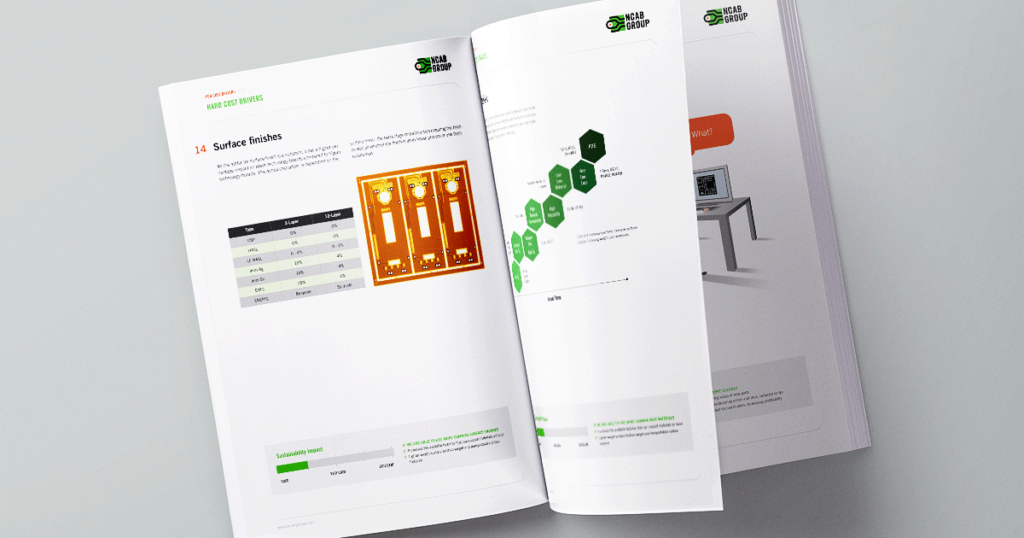
In our PCB cost drivers tool you can learn about the different factors that drives the cost of a circuit board, but also highlights how these factors in turn can impact the sustainability.

PCB cost drivers
What drives the cost of a circuit board? And how do those factors in turn impact the sustainability? To avoid large cost drivers we have developed a tool that can support you.
Local support –With a global presence and an extensive network of local offices and representatives, we offer personalized assistance and expertise in various regions. Through our local support, we ensure clear and efficient communication. Our knowledgeable teams understand the specific requirements and challenges of each market, enabling them to provide tailored solutions and valuable guidance throughout the PCB manufacturing process.
Key specifications for reliability – We have our own bespoke PCB specification that is used for all PCBs that we supply to customers. Several important PCB features specified are unique for us and/or go beyond the industry standard IPC Class 2. This is one of the factors that make it possible for us to provide a more reliable product than many of our competitors.
As electric vehicles continue to revolutionize the transportation industry, the importance of electric vehicle charging infrastructure becomes paramount. And printed circuit boards play a crucial role in ensuring the efficiency, reliability, and safety of EVC systems. As the EVC industry continues to evolve, we too need to adapt and learn, so that we can provide innovative solutions and comprehensive support to meet the evolving demands of the market.
