What is Ultra HDI PCB?
To be defined as an Ultra HDI PCB, the circuit board must have:
- Conductor width and isolation distance below 50 µm
- Dielectric thickness below 50 µm
- Microvia diameter below 75 µm
- Product characteristics that exceed the existing IPC 2226 level C standard
Learn more about Ultra HDI in this video.
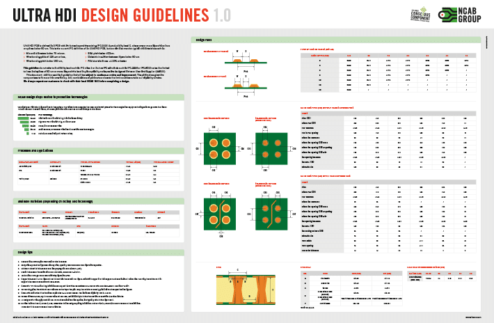
Design guidelines for ultra HDI
Download our PCB design guidelines for Ultra HDI to get your design right from start.
More information about Ultra HDI PCBs
Are there different types of HDI features?
The graphic below shows the main structures – type I, type II and type III as defined in IPC-2226.
Type I. Defines a single microvia layer on either one or both sides of core. Uses both plated microvia and PTH for interconnection, employing blind, but not buried vias.
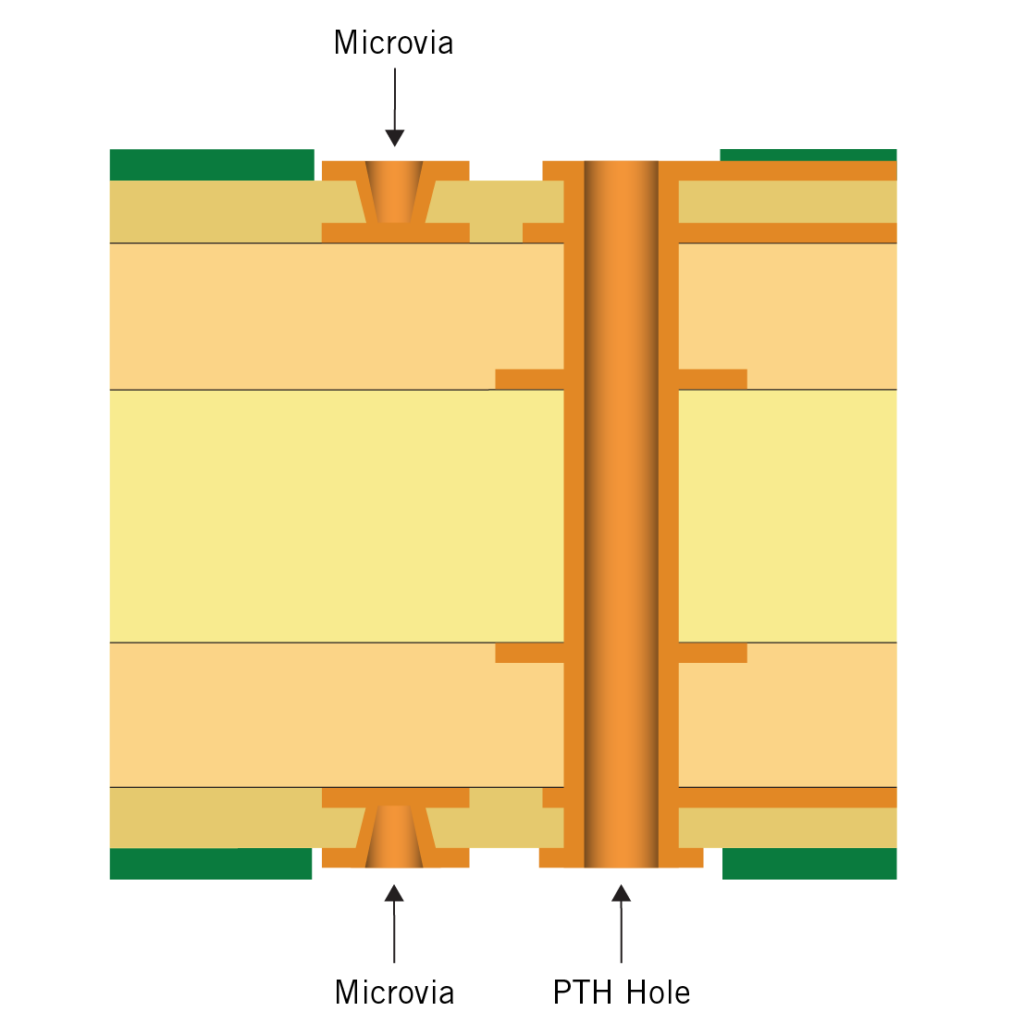
Type II. Defines a single microvia layer on either one or both sides of core. Uses both plated microvia and PTH for interconnection. Employs blind and buried vias.
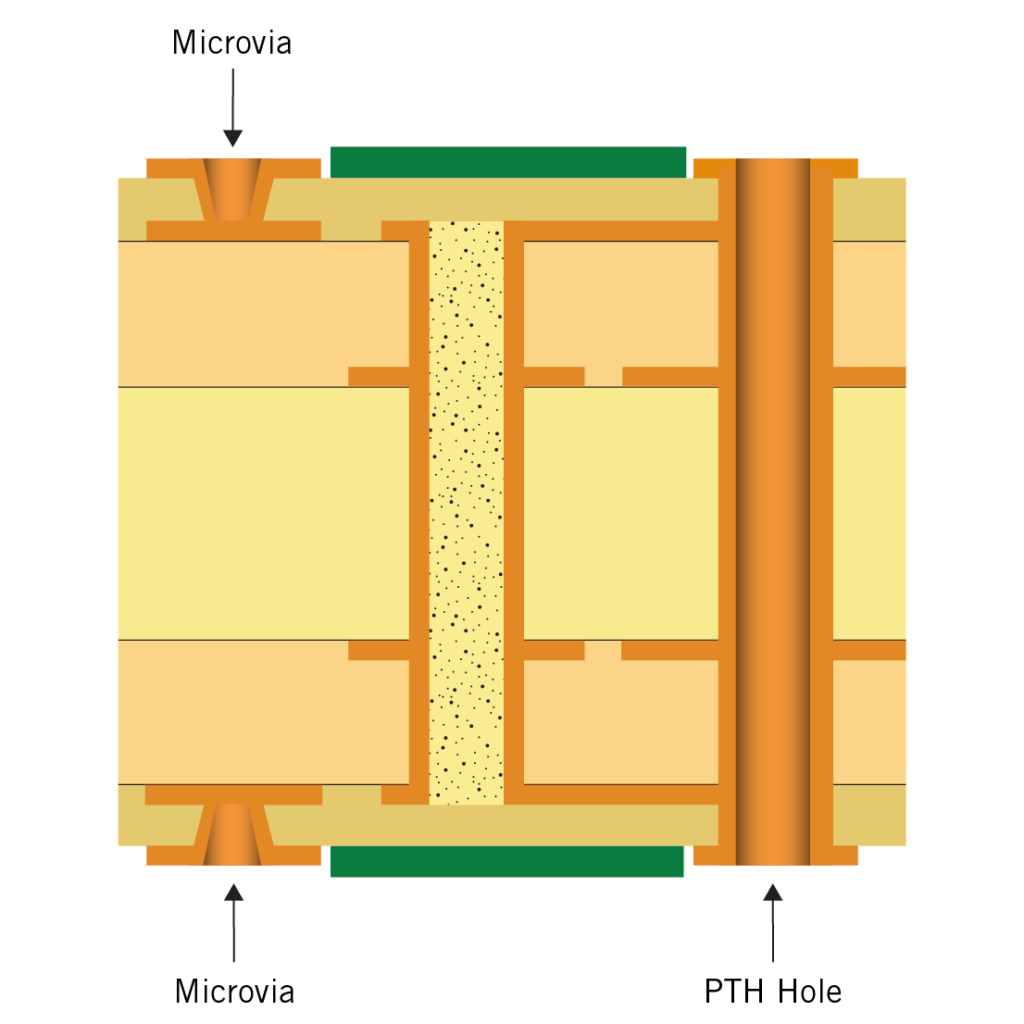
Type III. Defines at least two layers of microvia on either one or both sides of core. Uses both plated microvia and PTH for interconnection. Employs blind and buried vias.
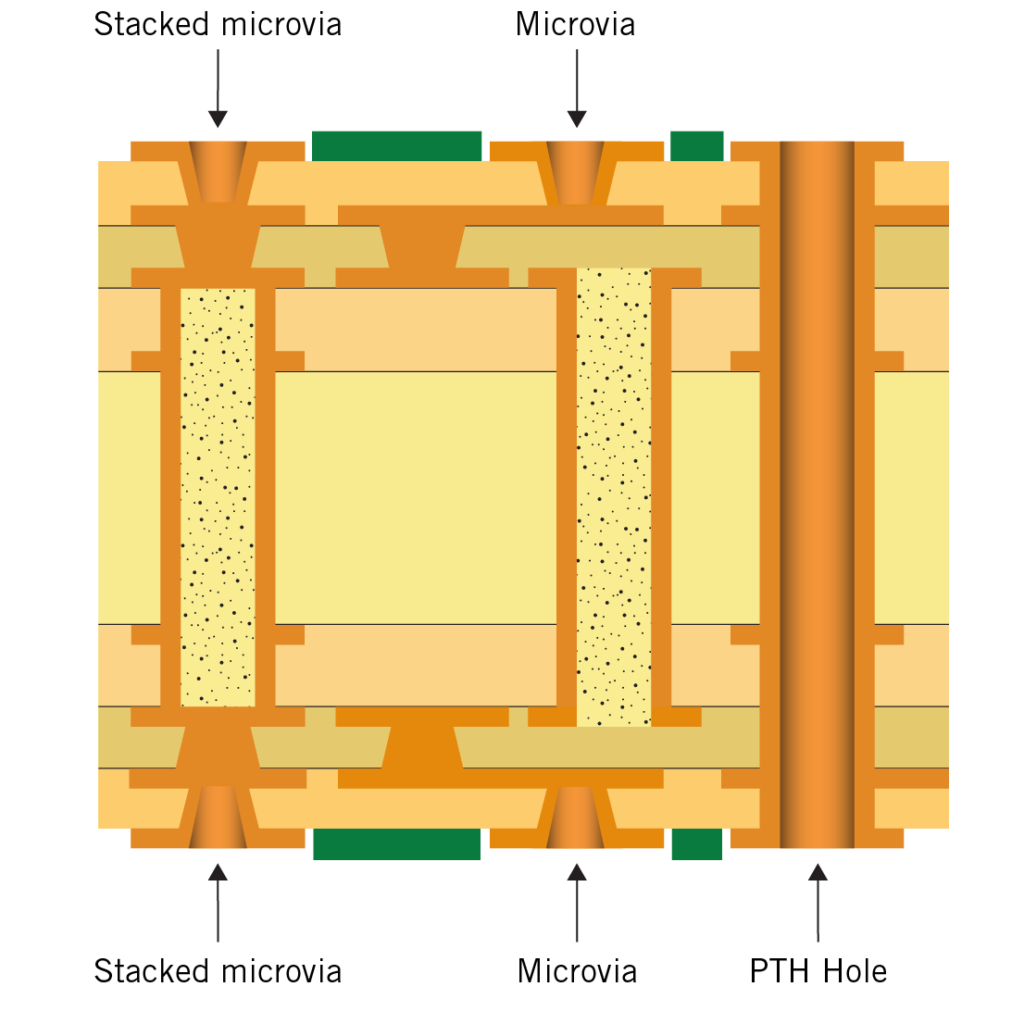
Construction terminology to define the degree of HDI construction:
- 1+n+1 = single layer of microvia (as per the type I and type II examples above)
- 2+n+2 = 2 layers of microvia (as per the type III example above)
- 3+n+3 = 3 layers of microvia
Learn more about HDI PCBs
What is a HDI PCB?
IPC-2226 defines HDI as a printed circuit board with a higher wiring density per unit area than conventional printed circuit boards (PCB). They have finer lines and spaces ≤ 100 µm / 0.10mm, smaller vias (<150 µm) and capture pads <400 µm / 0.40mm, and higher connection pad density (>20 pads/cm2) than employed in conventional PCB technology.
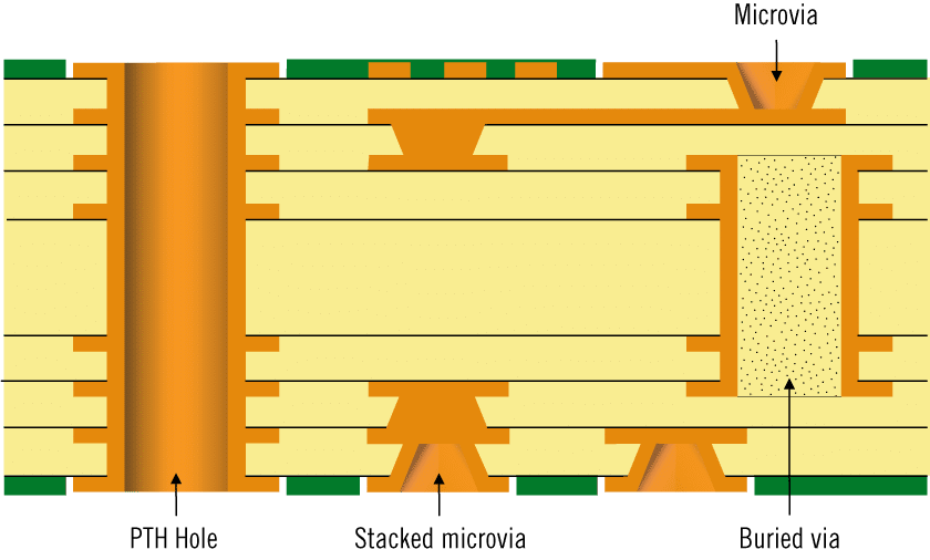
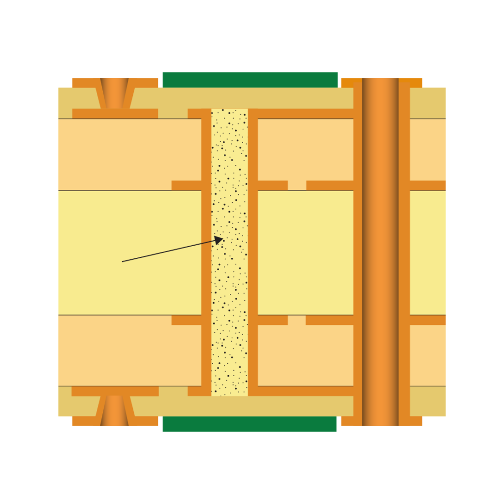
What is meant by a buried via hole?
This is a hole that runs between one or more inner layers. They are normally mechanically drilled.
Would you like to learn more about microvias?
What is meant by a blind via hole?
A blind via hole is a hole that runs from an outer layer to the inner layer, but not through the entire PCB. These holes can be drilled mechanically or using laser technology. The image shows a laser drilled blind via.

Would you like to learn more about microvias?
What is a microvia?

According to the new definition within IPC-T-50M a microvia is a blind structure with a maximum aspect ratio of 1:1, terminating on a target land with a total depth of no more than 0.25mm measured from the structure’s capture land foil to the target land.
The IPC-6012 also defines the structure of a Microvia.
- The Microvia is a blind structure with a maximum aspect ratio of 1:1 between hole diameter and depth, with a total depth of no more than 0.25 mm, when measured from the surface to the target pad or plane.
- Typically NCAB considers the dielectric thickness between surface and reference pad to be 60 – 80um.
- The diameter dimensions of the microvia have a range of 80-100 microns. The typical RATIO is between 0.6: 1 to 1: 1, ideal 0.8: 1
