
PCB material selection in high-speed and RF designs
Effective material selection requires a structured approach, supported by verified data, repeatable test methods, and clear documentation aligned with IPC standards.

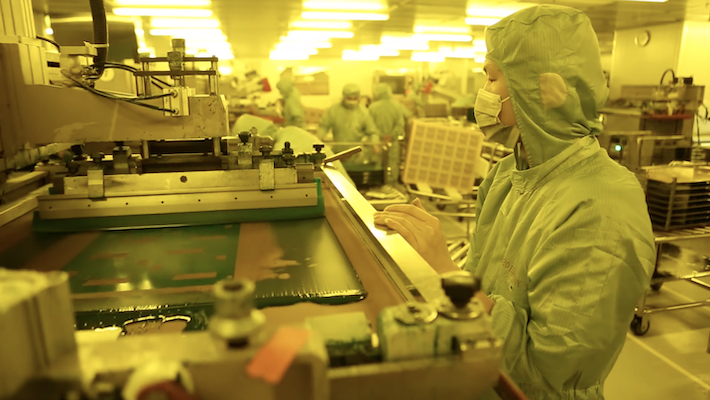
PCBs for medical devices – where the real supply chain risk hides
Reduce PCB supply chain risks through early collaboration, clear documentation, factory oversight, and sustainable sourcing from design to final product.

Tabbed routing in high-speed DDR PCB designs
Tabbed routing is a design method for scenarios where PCB routing space is limited. It is widely used in high-speed DDR PCB design.

Avoiding DfM pitfalls: common design choices that complicate PCB production
DfM pitfalls within PCB design can increase production lead times and non-material costs. Learn how to avoid them.

HDI PCBs: Make the right choice from design to volume
Learn more about the key factors for a successful production of HDI PCBs.
PCB Solder mask
Learn about the complexities of PCB solder mask and equip you with essential insights for your manufacturing endeavours.

PCB Bow and Twist: Challenges, Causes, and Solutions
Bow and twist are two types of deformations that can occur in the PCB. Bow refers to there being an upward or a downward curve in the middle part of the PCB. Twist refers to there being one corner higher or lower than the other corners of the board.

PCB Requirements for the Aerospace Industry
The design and performance of the aerospace PCB, a key to all aerospace systems, must be impeccable. Learn more here.

PCB design for extreme environments
PCB design for extreme environments – challenges with thermal management, altitude and shock and vibration events.

PCBs for Harsh and Extreme Environments: What defines an extreme environment?
PCBs used in harsh and extreme environments will be exposed to extreme situations. Learn about what defines extreme environments and about the PCBs used.

PCB designs with high-power applications – demands and considerations
High-power applications are those that require a lot of power to operate. This is usually because they are used in devices that need to be able to run for a long time without being plugged in.
Semi-Flex PCBs vs. Flex PCBs
When choosing PCBs that can bend into place, electrical engineers have a choice between using flex and semi-flex PCBs. Following is a basic overview of how these two types of PCBs differ and their uses in modern electrical devices.

Via Hole Design – a cautionary tale
Imagine you are a start-up company. You spent a year designing a product from start to finish. You have built the prototypes; there were some snags along the way but ultimately, the end product is perfect. You’re finally ready for volume production. Once you use multiple suppliers pricing out your bare board, you discover there’s […]

HDI – high density interconnect PCBs – design trends
With a higher wiring density per unit area than conventional PCBs, HDIs require different designs. Here you can read about HDI PCB designs & trends.

Applications of PCBs – use field engineering experts on your design
Have your PCB supplier involved early in the design phase First, let’s discuss a resource like this. At NCAB Group, they are field application engineers (FAEs). The benefit here is an experienced field application engineer will have worked on many PCBs for a variety of applications and have the capability and knowledge to recommend […]
PCB Button Plating – what is it, when and why is it needed?
The term button plating refers to the visual aspect of the final product. If you were to look at the cross-section, you would see your flat surface and then you would have what looks like buttons as the PTH is slightly raised from the other copper features.

The changing world of PCBs
What impact will the upcoming technical trends have on the PCB industry? Chris Nuttall, COO NCAB Group gives his view about this.

Our technical team – always ready to support you
Jeffrey Beauchamp – Technical / Engineering Manager at NCAB Group USA Jeffrey has been with NCAB since 2003. What are your responsibilities as Technical / Engineering Manager?I am responsible for supporting our customers with technical guidance, mentoring and assisting our team of technicians across North America and qualifying and maintaining our Domestic supplier base. What […]

Soft cost drivers in PCB production
Soft cost drivers – an important factor That reason is whether your role is managerial, commercial or technical there is a good chance that you have an interest in ensuring that the printed circuit boards you are purchasing, designing or assembling are as efficient as they can be in terms of achieving what we […]

KTH Formula Student
Why is this project of interest for NCAB? “NCAB strive to fill up with new expertise in the field of technology and hence a broad recruitment base is needed. We want to attract all young people regardless of who you are and where you come from, both to encourage young people’s technological interest and at […]

Why your standard PCB fabrication notes needs updating
I’ve noticed that our clients are understanding more and more that PCBs are the key component, but still have challenges communicating to their PCB suppliers what they want to build. When we receive Gerber files for an order there are times we cringe because we’re missing pieces of information necessary to make sure the PCB […]

Understand RF PCB Design – view and solutions
Understand RF PCB design by reading how RF circuitry is today crammed into a large variety of commercial products.

