
PCBs for medical devices – where the real supply chain risk hides
Reduce PCB supply chain risks through early collaboration, clear documentation, factory oversight, and sustainable sourcing from design to final product.

PCB stackups: What designers need to know about prepregs
Learn about defining PCB stackups, the correct amount of prepreg layers needed to achieve the proper insulation thicknesses, etc.

Risk reduction in medical PCB supply chains
Hands-on lesson from real-world production and design experiences of medical PCBs.
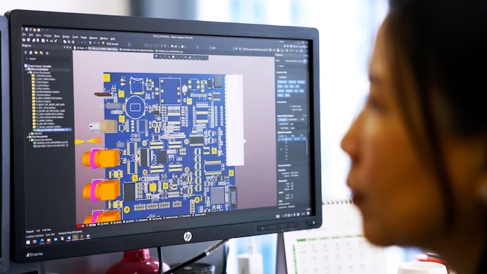
Avoiding DfM pitfalls: common design choices that complicate PCB production
DfM pitfalls within PCB design can increase production lead times and non-material costs. Learn how to avoid them.

The future of sustainable PCBs: Moving towards circularity
As businesses & regulators in the electronics industry push for greener solutions, circularity in PCBs has gained momentum.
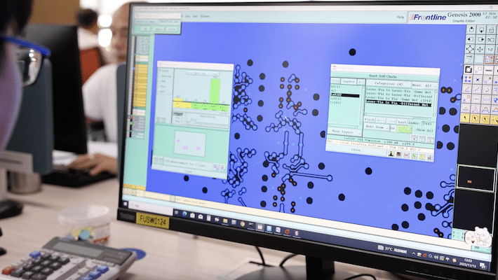
PCB Fabrication Drawing
Fabrication notes, Drill Table, Scaled Drawing, Stackup Drawing and Array Drawing are all parts of a PCB fabrication drawing. But – what is a fabrication drawing – and why do you need it?
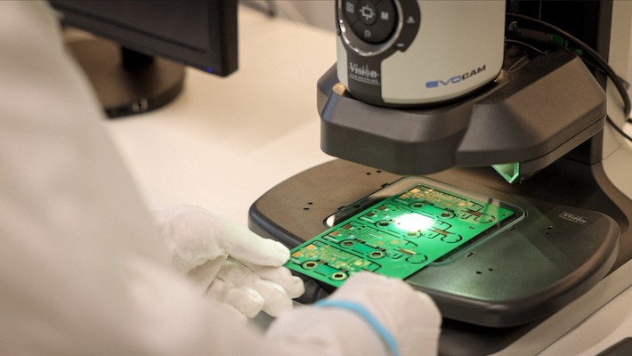
Manufacturing of PCBs for railway applications – four critical processes
When producing PCBs for railway applications it’s important to use the right parameters, equipment, and processes to ensure PCB reliability.
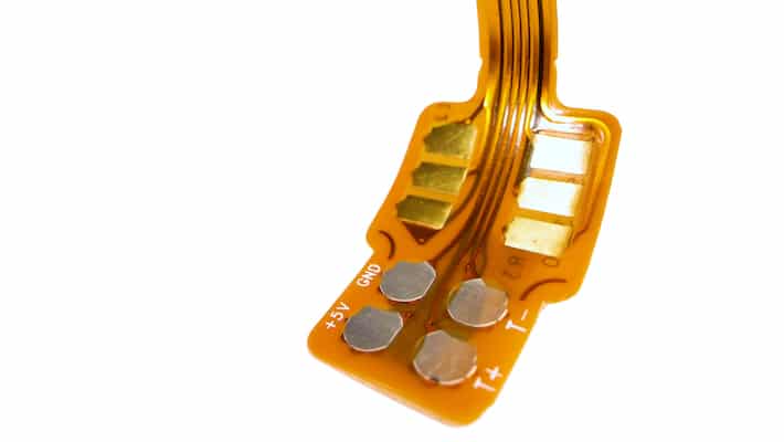
What is a PCB?
A PCB is built by non-conductive materials such as fiberglass or epoxy and has conductive pathways etched or printed onto its surface.

PCBs for Harsh and Extreme Environments: What defines an extreme environment?
PCBs used in harsh and extreme environments will be exposed to extreme situations. Learn about what defines extreme environments and about the PCBs used.

Data Matrix and QR Codes for PCB Information and Traceability
Data Matrix codes offers high data density in a very small size, making them an ideal solution for marking PCBs where space might be limited.
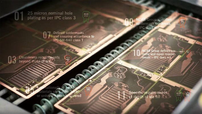
How an advanced product specification leads to reliable PCBs
Our PCB specification includes over a 100 different requirements or criteria, all of which must be met in the manufacture of PCBs for our customers – all to make reliable PCBs.
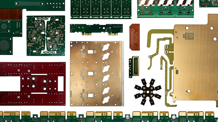
PCB Etchback Processes
PCB etchback is a process applied within to maintain optimized routing signals between multiple layers within printed circuit boards.

Electronics are transforming the world
Electronics trends in general and electrical vehicle charger in particular – learn more about important driving trends within electronics.
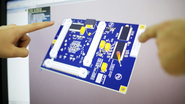
Via Hole Design – a cautionary tale
Imagine you are a start-up company. You spent a year designing a product from start to finish. You have built the prototypes; there were some snags along the way but ultimately, the end product is perfect. You’re finally ready for volume production. Once you use multiple suppliers pricing out your bare board, you discover there’s […]
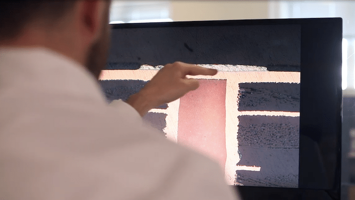
Via hole protection – what is it and when can it be used
Via hole protection is a PCB manufacturing technique in which the via hole is filled with solder mask or epoxy.
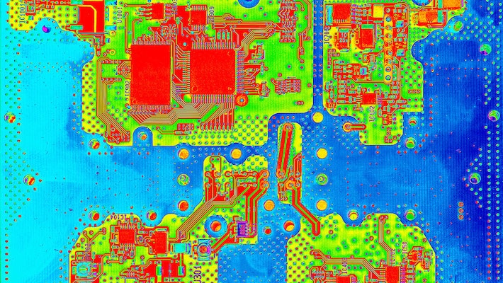
Thermal management in electronic systems is becoming increasingly important
In today’s electronics industry there are increasing calls for special thermal management solutions. NCAB’s experts tell about the methods available.

The road to sustainable operations
What is sustainability work all about in practice and how can businesses get to a point where they are making a real difference?

Soft cost drivers in PCB production
Soft cost drivers – an important factor That reason is whether your role is managerial, commercial or technical there is a good chance that you have an interest in ensuring that the printed circuit boards you are purchasing, designing or assembling are as efficient as they can be in terms of achieving what we […]

PCB standards – why do we need them?
Have you ever designed a board, but got feedback that it couldn’t be manufactured unless changes were made? Or maybe you’ve designed a complex board and sent it to the factory, only to find out that the manufacturer didn’t build the board to your expectations? Printed circuit boards are becoming more complex, the factory options […]

Key aspects for a reliable PCB
We know that good reliability is secured by achieving a good balance between verification on a product level and verification of the process. It cannot be achieved by screening or sorting on a product level – you cannot ‘inspect in’ good quality or reliability as the old adage goes. Classifications according IPC Class 1: General […]

NCAB Group – Making PCBs cool since 1993
Michael Larsson VP Sales, Group Function How would you describe a PCB to a child? It’s flat and often green, with a lot of small holes. You almost never see it, but it helps you get to soccer practice, keeps your ice cream cold and your Snapchat functioning. It make all the difference for […]


More design tips – get it right from the start
COMMON DESIGN PROBLEMS REGARDING HDI PRODUCTION PROBLEMS DEPENDING ON THIS BEST SOLUTION Too tight demands on the thickness of overplating of plugged vias. (POFV or VIPPO) Affects the flow of the process, at a reasonable thickness of the overplating all the vias can be drilled in the same operation, which makes the process much […]
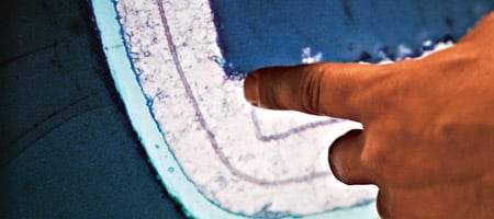
PCB DfM – a pathway to lower overall cost
It’s all about connections, not simply those that the designers make to define the circuit or the ones that circuit board manufacturers create to fab the PCB. It’s about connecting the design intent with PCB manufacturing capabilities and assembly requirements. Without these connections, the PCBA will not have the manufacturing robustness or process yield needed […]

CSR – an important issue for the future
Still there are differences between the environments our future generations grow up in – with our well appointed NCAB UK offices & warehousing based here in Wiltshire, in open countryside – it is a stark contrast to the industrial zones of southern China where many of the PCBs consumed by global electronics markets are made. […]
