No 2 2022
Ultra HDI PCBs put high demands on technology and manufacturing
MORE ARTICLES RELATED TO THE TOPIC:
Today’s electronics industry is characterized by a strong miniaturization trend. Components are getting smaller and smaller, which also places new demands on the design of the PCBs they are mounted on. NCAB Group is deeply committed to IPC’s work developing standards for ultra-dense Ultra HDI PCBs and will be in a position to deliver them to customers in 2023.
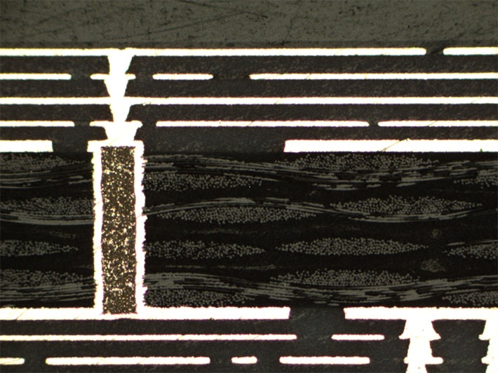
We find miniaturization in a steadily growing number of electronics applications. Today, for example, there are BGA (Ball Grid Array) components where extremely small conductor widths and minimal clearance on the circuit boards are prerequisites for use in designs that are even denser than on HDI (High Density Interconnect) circuit boards. With dielectric thickness and isolation clearances down to 50 µm, these boards used to be regarded as very dense.

“NCAB receives inquiries daily concerning printed circuit boards where the requirements are smaller conductor widths and isolation distances than on standard HDI boards.”
Jan Pedersen, Director of Technology, NCAB Group
“The highly miniaturized new components have been used, among other things, in technology for 5G telecommunications, sensors and in the major manufacturers´ high-end smartphones. We are now starting to see the technology spreading to other segments of the industry. NCAB receives inquiries daily concerning printed circuit boards where the requirements are smaller conductor widths and isolation distances than on standard HDI boards. Applications in medical technology and the automotive industry are a couple of examples.” explains Jan Pedersen, Director of Technology at NCAB Group.
What is an Ultra HDI PCB?
To be defined as an Ultra HDI board, the circuit board must have:
- Conductor width and isolation distance below 50 µm
- Dielectric thickness below 50 µm
- Microvia diameter below 75 µm
- Product characteristics that exceed the existing IPC 2226 level C standard
A lack of industry standards for Ultra HDI
The problem stems from the lack of industry standards regarding the design of these printed circuit boards and the performance and quality requirements they have to meet. Suppliers are responsible for the manufacture of Ultra HDI boards had been contracted at an earlier stage by major companies such as Apple, Intel, Samsung and the like. These players have invested heavily in the factories in question, making it difficult for others to gain access to the technology.

There are other factories that can manufacture PCBs with dielectric thickness and isolation distances below 50 µm, but are unable to go all the way down to really small distances of, say 20-25 µm, that may be required today. In a move to remedy the problems and create an appropriate and well thought-out industry standard, the industry body IPC set up a task group for the new type of technology, which they eventually named Ultra HDI. Jan Pedersen is chairman of the group.
“I was chairman of the IPC’s medical committee, where we discussed the issue of new requirements and parameters. That discussion gradually evolved and eventually led to the formation of this working group. Over the past three years, the group has been working on developing a new IPC standard for what we now know as Ultra HDI motherboards. We have produced a document that serves as a guide to build design and production standards for these boards,” says Jan Pedersen.
“The highly miniaturized new components have been used, among other things, in technology for 5G telecommunications, sensors and in the major manufacturers´ high-end ‘smartphones.“
Jan Pedersen, Director of Technology, NCAB Group
Major investments needed
Ultra HDI PCBs are defined as products with conductor widths, isolation distances and dielectric thicknesses under 50 µm, microvia diameters of less than 75 µm and characteristics that exceed the existing standard IPC 2226 level C. To enable factories to manufacture Ultra HDI boards, a great deal of updating needs to be done. Investments have to be made at the manufacturing stage, in both equipment and processes.
Developments were previously characterised by a ´chicken-or-the-egg problem`. The factories couldn’t obviously produce something that the customers didn’t know how to design, and the customers were not able to order components that the PCB factories couldn’t make. In order for the factories to be able to build their capacity, they first need to base their manufacturing on a standard for the PCBs. With the guidance that the IPC working group is releasing during autumn, the industry will have a common standard blueprint to work from.

Internal work to support the factories
– At NCAB, a special group in our internal technical council is working to support our factories to build capacity to meet the Ultra HDI requirements. An important method is the so-called mSAP (modified Semi-Additive Processing), where copper is built up on a thin initial layer instead of being etched off a thick layer. It is also better for the environment, since less copper is used. Some factories are already able to do this up to a certain limit.” says Jan Pedersen.
The greater level of miniaturization also requires that the pattern can be transferred to the board with a sufficiently high resolution. The factory needs to have cutting-edge so-called LDI equipment (Laser Direct Imaging). Moreover, the environment has to be extremely clean to avoid contamination and dust and this entails considerable investment. Testing processes and automated optical inspection (AOI) equipment also needs to be updated to detect and avoid potential board defects. Likewise, you have to look at the equipment and the chemistry when copper plating. Miniaturization will also generate a need for cleaner and more homogeneous materials.
“For NCAB’s work in supporting the factories, it is of course an advantage that I have headed the IPC task group and thus have valuable insight into the challenges of Ultra HDI. Our factories, especially those in China, are now fully committed to growing their capability and we expect them to start delivering Ultra HDI boards in 2023.” explains Jan Pedersen.
Updates required for manufacturing Ultra HDI circuit boards
PCB factories that take on the manufacture of Ultra HDI boards will need to meet more stringent requirements with regard to equipment and manufacturing environment.
- State-of-the-art LDI equipment
- Extremely clean environment
- More thorough testing
- Latest automatic optical inspection equipment
- The latest equipment and chemistry for copper plating
- New methods such as mSAP
- New, cleaner and more homogeneous materials

What is the task of NCAB Group’s Technical Council?
As Director of Technology, Jan Pedersen heads NCAB’s internal technical council. This brings together 60 technicians from the organization’s local companies.
A number of smaller focus groups have been formed within the council – 13 so far – to build up specialist knowledge in, for example, different technologies and to tackle diverse needs within the industry. One of these focus groups is the Ultra HDI group, which is currently working with NCAB’s PCB factories to enable them to meet the miniaturization requirements. Jan Pedersen highlights two more groups that can add a lot of value to NCAB’s customers.
“One is building and documenting common technical questions that our Factory Management department receives from our partner PCB factories. The questions are directed to our customers and are typically about issues such as designs that the factories have found unsuitable for manufacturing. We are now compiling all this into a training document that customers, factories and we at NCAB can learn from. The document allows customers to learn more about board designs, and on the supplier side, it can help us become better at handling various issues.” Jan says.
Technology and process choices can reduce environmental impact
The second focus group Jan mentions is recently-launched focussing on sustainability. This group examines the extent it is possible to take into account and work out the impact on sustainability of various technology and process choices linked to PCB production.
“Sustainability is very important to us at NCAB. That´s what is driving us to help our customers make informed decisions that also include a sustainability perspective. For example, it could involve us describing to a customer the environmental impact of moving from a 6- to a 12-layer board. We are now looking for ways to quantify and make these types of factors measurable, which would be something completely new in the industry.” concludes Jan Pedersen.


