HDI – High Density Interconnect PCBs
This, combined with our worldwide technical organization, bring a comprehensive knowledge of the requirements and manufacturing methods required for successful HDI products. Learn more about our technical specification for HDI PCBs, how IPC defines a HDI board and get some design tips.


What defines a HDI board?
IPC-2226 defines HDI as a printed circuit board with a higher wiring density per unit area than conventional printed circuit boards (PCB). They have finer lines and spaces ≤ 100 µm / 0.10mm, smaller vias (<150 µm) and capture pads <400 µm / 0.40mm, and higher connection pad density (>20 pads/cm2) than employed in conventional PCB technology. There are different types of HDI features, type I, type II and type III.
The different types of HDI features
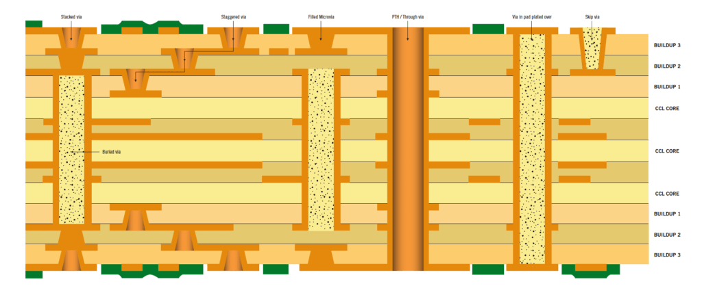
The graphic below shows the main structures – type I, type II and type III as defined in IPC-2226.


Construction terminology to define the degree of HDI construction:
- 1+n+1 = single layer of microvia (as per the type I and type II examples above)
- 2+n+2 = 2 layers of microvia (as per the type III example above)
- 3+n+3 = 3 layers of microvia
Our technical capabilities for HDI PCBs
For information about our technical capabilities for HDI PCBs, read more at our Technical Capability page. You will also find information relating to materials, other PCB technologies or product types which we currently produce, as well as some of the tolerances which we can achieve.
What you need to know about design and HDI PCBs
Below you can learn more about different aspects of design and HDI PCBs like design tips, design guidelines and design trends.
Design tips for HDI PCBs
Nothing affects the PCB’s cost and quality as much as the initial design. Here you find some useful information about common design problems, what production problems they can cause – and most important – the best solution to avoid them!
| COMMON DESIGN PROBLEMS REGARDING HDI | PRODUCTION PROBLEMS DEPENDING ON THIS | BEST SOLUTION |
| Dielectric too thick for laser vias | – Increased time for laser drilling, lower productivity. – High risk for voids in the plating process, especially in the bottom of the microvias. – Increased price for the PCBs due to reduced yields. | Use an aspect ratio under 0.8:1. |
| Too small microvia size | – Increased risk for the microvia to be blocked by unknown material and therefore won´t be plated satisfactorily. – High risk for poor plating of the microvia, especially in the bottom. – Increased price for the PCBs due to reduced yields. | – Use microvias of 100 μm with an aspect ratio under 0.8:1 for microvias intended for copper filling. – Use microvias of 125 μm and with an aspect ratio under 0.8:1 for microvias where copper filling is not a requirement. |
| Too tight geometries in the form of too small capture and target lands for the microvia | – If the target land is too small, the risk will increase for partly missing it (so called overshoot), and material adjacent to the pad will be burnt down to the next layer. – If the capture land is to small, it is a risk for the land to be broken, which is not acceptable to any class in IPC-6016. | If possible, use a start pad that is 200 μm larger than the microvia. At tighter geometries consult NCAB. |
| Too tight demands on permitted dimple on copper filled microvias | Increased price for the PCBs due to reduced yields. | Place the requirement of dimple to a maximum of 25 μm. |
| Too tight demands on the thickness of overplating of plugged vias. (POFV or VIPPO) | Affects the flow of the process, at a reasonable thickness of the overplating all the vias can be drilled in the same operation, which makes the process much easier. If the overplating is too thick this will reduce the possibilities to produce outer layers with thin tracks/small isolation. | Set the requirements according to IPC-6012 class II and demand only ≥ 6 μm as overplating thickness. |
| Epoxy via plugging demands for too many different sizes of vias, this applies to both buried as for through vias | Hard to control that bubbles don´t occur in the final plug, and that there won´t be a problem with complete filling. | Only one size of the plugged vias are preferred, if more sizes have to be plugged, keep them within a range of 0.15mm. |
| Microvia placement | If microvias are placed directly into SMD surfaces, unnecessarily voids can arise in the solder joints at reflow soldering. The price structure increases if the microvias are copper filled. | Pull the microvias from the SMD surfaces if possible. If there is no place to do alternative 1, place the microvias right into the pad and demand for them to be copperfilled. |
| Too small distance between the staggered holes and the microvias – microvias or microvias – buried vias | If the staggered microvias are placed too close to each other, there is a risk that the overlaying hole can intrude on the underlying one with bad plating as a consequence. This can be solved by copper filling of underlying microvias or overplating if buried vias, all this means increased cost and risk. | Regarding microvia-microvia, keep a distance of 0.30 mm between holes if possible, if not, go down to 0.25 mm. Example: 0,10 mm microvia and 0,25 mm buried hole gives 0,475 mm and 0.425mm in center to center distance.
|
Don´t hesitate to contact us if you need help with your PCB design – we are happy to help!
Design guidelines for HDI PCBs
More than 30% of the Gerber data we receive do have some issues. They can contain ambiguous information, errors, design rule conflicts, missing information and contradictions between the data and specifications. To prevent that it gets wrong from the start, we have put together our design guidelines, to use as a checklist. This is an extract from our PCB design guidelines for HDI PCBs.
The whole design guideline can be downloaded for free.
Minimum track and gap for cap plating
IPC-4761 TYPE VII PLUGGING / VIPPO / POFV

* Valid only for the outer phase of a buried core which needs cap plating – typically when a microvia is stacked on a buried hole.
** For design tighter than this, please consult your local NCAB technical contact to review specific projects case by case.
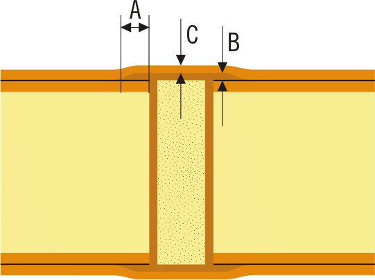
B. Minimum copper wrap thickness 5 um for class 2 and class 3
C. Minimum cap plating 12 um for class 3, minimum cap plating 5 um for class 2
We not only have design guidelines for HDI PCBs, but also for Multilayer PCB, Ultra HDI PCB, Flex / Rigid-Flex PCBs, Semi-Flex PCB, Copper coin, Via Protection and Stackups and Impedances.
Blog posts about HDI
In a couple of blog posts we have delved into the key factors for a successful production of HDI PCBs, and scrutinized design trends for HDI PCBs. Read an excerpt below.
Design trends for HDI PCBs

The miniaturization of electronic components pushes the evolution of printed circuit boards towards complexity that was unthinkable only a few years ago. The circuit boards needs more functions and performances all while being thinner and lighter. This requires a very rigorous design and production process. To develop this type of circuit boards, we need solutions for a greater density of connections and more layers in the printed circuit board.
The increasingly narrow design means less space available for routing, which results in thinner tracks and gaps with through holes of increasingly smaller diameter.
A couple notes on HDI designs:
- Blind holes are laser holes on the external sides
- Buried holes are laser holes to connect intermediate layers
- We also need thinner pre-preg and CCL laminates than conventional multilayer products
When the project is being taken to extremes, it is clear that the entire design process must follow some necessary guidelines, from the designer to the PCB supplier.
HDI PCBs: Make the right choice from design to volume
There are two key factors for the successful production of HDI PCBs: first, making the right choices at the design stage, and then carefully choosing the factory that can support the specific technical demands of the project.
Whether it’s consumer electronics, computers, automotive or medical technology, the overall trend is reduction in size. Not just through a reduction in actual or finished product size, but also as the components themselves are becoming smaller, so the assemblies must be more densely packed and use smaller features.
The onset of these increasingly sophisticated electronic products has led to more advanced PCBs becoming more commonplace. The specifications here require high-density interconnect (HDI) solutions with greater number of layers, and more connections both on the surface and inside the PCB, utilizing finer conductor widths and narrower spaces between them.
The increased number of layers, together with the microvia technology, also requires the use of thinner prepegs and cores than in conventionally manufactured boards which also leads to increased demands upon the factories.

Download our HDI PCB design guidelines
Use our design guidelines to get your PCB design right from the start.

Contact us
Please contact your local NCAB Group company if you need further information or assistance, we are happy to help you.